Continue to Site

Welcome to our site!

Electro Tech is an online community (with over 170,000 members) who enjoy talking about and building electronic circuits, projects and gadgets. To participate you need to register. Registration is free. Click here to register now.

  • Welcome to our site! Electro Tech is an online community (with over 170,000 members) who enjoy talking about and building electronic circuits, projects and gadgets. To participate you need to register. Registration is free. Click here to register now.

Couldn't turn on and off the logic MOSFET....

Status
Not open for further replies.

devonsc

New Member
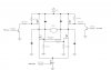
Do you guys mind to comment about this? I tried to turn on the mosfet by doing the following. With the circuit as shown constructed, I measure the voltage drop across the Drain and Source and I obtain 5V. But I'm not sure if Im doing the right thing as even though I remove 5V to the Gate, I still obtain a reading of 5V if I were to tap my multimeter on the Drain and Source...

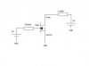
Mind to comment about this? Please? Is it trut that I'm suppose to read any values if I remove the 5V source for the gate?

By the way, the MOSFET used is a logic MOSFET, IRL2703.
 

Attachments

  • mosfet_971.jpg
    mosfet_971.jpg
    9.4 KB · Views: 2,165
well of course ur gonna get a reading if you're putting your multimeter's leads on the drain and the source. just remove the fet and you are just measuring that battery voltage w/ the 1k resistor in series with the positive of the battery. take a look @ the picture.
 

Attachments

  • mosfet_971.jpeg
    mosfet_971.jpeg
    11.5 KB · Views: 1,205
Aikss...but if I were to try simulating it, I will obtain approximately 0V across the FET if I were to tap the voltage in the same manner....

By the way, if what I have in mind is totally wrong, do you mind guiding me how should I check or try out to switch the on/off of this logic MOSFET?

Thanks in advance...
 
devon . . . im sorry :oops: , actualy u r right. that WILL work :oops: :oops: :oops: :oops: :oops: :oops: i jumped the gun :lol:

i was forgetting that wen the FET is on, its like shorting to ground and therefore no voltage potential.

well, i see no reason why your circuit should not work. the only thing i can think of is that the voltage @ the gate is too high. on a FET that i was working w/, the maximum gate voltage was only like 4v.

VERY quickly, short the gate and the drain and see if this makes it turn on. if it doesnt, it might be shot.

also, the pinout on the FET is probably different from your regular ol' npn or pnp transistor, so beware of that. i forgot about that the first time i tinkered w/ FETs.
 
the only thing i can think of is that the voltage @ the gate is too high. on a FET that i was working w/, the maximum gate voltage was only like 4v.

yeah but the MOSFET with which he is working with has a maximum gate to source voltage of 16V. and he is only applying 5V so that isnt a problem.

i would agree with you about the pin configuration. maybe devonsc has swapped two pins. check the datasheet and then make your connections
 
yeah but the MOSFET with which he is working with has a maximum gate to source voltage of 16V. and he is only applying 5V so that isnt a problem.

it was the best i could come up with :lol: . i just fried a FET cuz there was like 12v @ the gate (i thot it was higher)
 
Can anyone tell me how does a MOSFET overheat?
Im currently attempting this circuit(U dont have to laugh at my circuit. i know its very lousy and crude. it has already been criticized. but since im using low current, it was ok). By placing 5V to the Mosfet , everything is fine. The motor works great. However, when i input PWM pulses into the mosfet( logic level mosfet), it heats up very very quickly.
Anyone knows why the pwm pulse can overheat it?
 

Attachments

  • mosfetwhy.jpg
    mosfetwhy.jpg
    27.9 KB · Views: 1,146
fabbie said:
Can anyone tell me how does a MOSFET overheat?

A MOSFET is no different to anything else, it dissipates heats based on volts x amps - W=VI.

When a MOSFET (or a transistor) is turned fully ON, it passes high current but only has a low voltage drop, so W is low. When it's turned OFF, it passes no current, but has a high voltage across it - so again, W is low.

If it's not turned on fully you get high current and high voltage, and the device (whatever it is!) gets hot. In switching circuits the speed of switching is critical, as the device will dissipate heat as it switches, so a slow switching speed will over heat the device.

I would suspect you either aren't switching the FET's on properly, or you aren't switching them fast enough - most probably the first option!.
 
I am guessing that the left and right PIC input signals are complements of each other - only way it will really work


The chances are it is overheating when you are PWMing it due to shoot-throughs.

If you look at your top FETS they have a 1k gate resistor to turn them off (slowing down their turn-off time)

you want Fast off and slow on when dealing with H-bridges (or have dedicated interlocks, which is better)

If I number the switch:
1...3
4...2


Say the Left PIC input is HIGH: This means that

FET-1 & FET-2 is on
FET-3 & FET-4 is off
ie current left to right through motor

At a PWM edge where Left PIC input goes from HIGH to LOW and Right PIC input goes from LOW to HIGH:


FET-1 gate is now being pulled highby a 1k resistor (high value slows down swithcing - in this case slows turn-off)

Meanwhile FET-3 has had its gate pulled hard down to 0V via a 100Ohm resistor (via a BJT) This is a FAST-ON !!!!!. This puts the source at the rail voltage. This voltage now feeds FET-4 via the 1k off resistor of FET-3 - Slow-on

Thus we have a slow off of FET-1 and now a slow-on of FET-4 at the same time (is) thus there is a high possiblity of a shoot-though (more likely a soft shoot-through with the FET's in their active region)


The same will happen for the other FET's and equally for a LOw to a HIGH.

Sucha shoot-though looks inherent with this design (I never liked those 1k resistors for gate resistors)
 
Try this
 

Attachments

  • h-bridge.png
    h-bridge.png
    9.3 KB · Views: 1,097
I think the two top P devices in the diagram should be flipped in the Y direction. The way they are drawn at the moment will have their drains to the +ve supply and the integral diode will be upside down conducting all the time.

Also make sure that if you are still going to use logic level devices that you need to swing the gate signal under 1V away from the +ve supply where the source is connected to, to turn off the device with this circuit. Maybe not a bad idea to have the push-pull drivers and pre-driver running off a slightly higher supply like 15V, to make sure there's no turn off problems. Should still be OK, as logic level devices can handle 20V
 

Attachments

  • p_fet.gif
    p_fet.gif
    1.9 KB · Views: 1,063
Well spotted TheOne.

Using a new CAD program and forgot about the flip on the P-types
 
But I just realized that there's a bigger problem looking at it more carefully. The devices will be on at the same time, red current spike.
 

Attachments

  • short_i1.gif
    short_i1.gif
    15.6 KB · Views: 1,034
That is why I really didnt want to put actual resistor vaules to the gate-drive (the 1k and 10R)

That will be dependant on the FET's being used. Since I do not know the generation of FET or more importantly the gate-charge of the FET I couldn't spec.

With your simulation you will proably see that shoot-through happening when the P-type turns off and the N-Type turns on (and maybe to a lesser extent then N-type turns off and P-type off).


With the higher gate capacitance on the P-type, the 1k is probably too low to turn it off.


Since this is a low voltage/low power H-bridge (a higher power would use dedicated interlocks) - could you find out what the gate capacitance of hte P-type is, compare against the N-Type.

The difference in capacitance, use that value (or closes standard value) and put a capacitor of that value in parallel with the N-Type gate terminal (across the Gate-Source)


IF you remember the original problem Fabbie only had 2 pins on a PIC to use. Delaying the switching of the FET's via it's gate-charge is an ok hack, but really you need dedicated interlocks. You really need a dedicated drive signal (and thus gate-drive) per FET/IGBT. Since Fabbie is resitricted, this approach is good BUT it must be turned for the FET's being used

Re-try with an xtra cap
 
Updated...
 

Attachments

  • h-bridge_824.png
    h-bridge_824.png
    9.9 KB · Views: 1,081
TheOne said:
But I just realized that there's a bigger problem looking at it more carefully. The devices will be on at the same time, red current spike.


Eqaully TheOne this was inherint in the previous design (if not worse) and is why I mentioned the heating of the FET's probably due to shott-throughs in a leg.

My approach with appropriate tuning (with limited control signals) will remove the shoot-throughs
 
sorry for the late reply ( is the forum server giving problems? cant seem to log on)

Im not really good in my electronics, my looking at the new circuit u guys pain-stakingly posted, please inform me if im wrong about this.

When LEFT pic input is HIGH, Q1 would be ON. While RIGHT pic input is LOW, Q4 is ON. Then, current flows from left to right.

If LEFT PIC and RIGHT PIC is LOW, are both Q3 and Q4 ON? (pls correct me about this, i thought that this wasnt allowed for H-bridges)

Furthermore, im limited to a single PWM channel Another thing to note is I would be using standard mosfets except for the logic level mosfet i posted earlier located at GND. Is putting a Logic level mosfet at the GND an unwise move?

LAstly, in the circuit u proposed, i dont get this part. What is this for?
THX alot. u guys are great help
 

Attachments

  • dontknow.jpg
    dontknow.jpg
    7.7 KB · Views: 1,051
The only condition in a H-bridge that are not allowed is a leg being on (IE a shoot-through)

That is
Q1 and Q4
or
Q3 and Q2

as I have numbered them


When the Left input is HIGH and the Right input is LOW
Q1 is ON and Q2 is ON thus current left to right

When the Left input is LOw and the Right input is HIGH
Q3 is ON and Q4 is ON thus current right to left.

As you can see the driving signal is the compement of each other. So you only have one PIC output available, just use a trasistor as an invertor to make the complement.


No for the case that you mentioned when both inputs are HIGH, then
Q1 and Q3 are ON (other 2 are off) All this is, is a zero-volt loop around the motor via the top switches/diodes

Equally if both inputs are LOW then Q4 and Q2 are ON and you have a zero-volt loop around the motor via the bottom switches/diodes.


Now there will be a problem (during powerup) IF you decide to use an iverter to generate the compment PWM. BUT if memory serves me correctly you had one PIC output to drive a disconnect/disable FET. This is not needed anymore and thus you can use that output to drive the other H-bridge leg and in the PIC code have a bit of cod ethat for diable output both as LOW.


As to the final point about what is the battery and the 100mF cap. It is exactly that.

You said this wat to run form a battery (or some other voltage source) that I assume you can discconect via a swithc somehwere. However, you still need a DC-link cap. For the acceleration and the sudden changes in load the battery probably wont be able to source all the charge, the cap acts as a firmer source - has to very close to the H-bridge.

Probably doesnt need to be a big as 100mF but suitablly sized for the ripple current that you will be seeing
 
Styx said:
Now there will be a problem (during powerup) IF you decide to use an iverter to generate the compment PWM. BUT if memory serves me correctly you had one PIC output to drive a disconnect/disable FET. This is not needed anymore and thus you can use that output to drive the other H-bridge leg and in the PIC code have a bit of cod ethat for diable output both as LOW.

Sorry. But i dont get what u mean. The circuit proposed has only 2 inputs. If i intend to drive the H-bridge using PWM, i would definitely require 2 channels. One for each input. Mind explaning again??
Did i mention that i was using the PIC's PWM? Although my PIC has already 2 channels, my plan was to design a H-bridge that only requires 1 channel. (something like the L298 chip).
That was why i connected the PIC PWM directly to the logic level MOSFET. But it failed to work.
 
Status
Not open for further replies.

Latest threads

New Articles From Microcontroller Tips

Back
Top