Continue to Site

Welcome to our site!

Electro Tech is an online community (with over 170,000 members) who enjoy talking about and building electronic circuits, projects and gadgets. To participate you need to register. Registration is free. Click here to register now.

  • Welcome to our site! Electro Tech is an online community (with over 170,000 members) who enjoy talking about and building electronic circuits, projects and gadgets. To participate you need to register. Registration is free. Click here to register now.

Conducted EMC failure for 1W Buck converter...shield the switching node with PCB copper?

Status
Not open for further replies.

Flyback

Well-Known Member
Hello,

Please help us to pass conducted emissions of EMC testing, particularly with reference to common mode noise created by the switching node of our 1W Buck converter

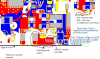
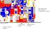
We have a 1W Buck converter (bias supply) on our offline 150W LED driver PCB (which uses linear current regulators).

It firstly failed EMC due to having the Buck’s switching node copper layed out all over the bottom PCB layer, where it was next to the earthed heatsink. (common mode emissions).

We now have removed the switching node copper from the bottom layer. However, do you believe that we should shield the switching node copper (which is now only on the top layer) from the earthed heatsink by putting some “quiet node” copper underneath the switching node of the Buck, in order to shield the switching node from the earthed heatsink on which the PCB sits?

(eg we could put the “quiet node copper” on middle and bottom layers of the 4 layer board. The switching node copper is now only on the top layer. The PCB sits on a thin thermal pad which is on the earthed heatsink)
 
Yes, the capacitive coupling from the switching transistor and nodes should be minimized as much as possible from the earthed heatsink.
A ground plane should significantly reduce that coupling.
 
Thanks, some say though that the switching node could induce noise into the ground plane if the ground plane is directly beneath the switching node?
 
Current pulse onto ground plane does not know what direction the source is, it goes all directions even producing a field at that point as EMI. Large as possible ground plane favored aiming towards the source or supply common connection point would be best.

Noise can occur independent on the type of switch used.

Inadequate plane trace size and thickness can cause noise.

How many via must the path transition though as each can add small capacitance on 2 factors,

1. DC, line charge capacitance.

or

2. A/C switching frequency, delays dependent on current value as each via can act as a minor choke (unless in grouped formation in numbers = reduction of issues), hard turns for current to take / zig zags slowing down the transition and adding noise, power transfer on ground trace in that case can yield impedance change from the switch peaks alone if the plane is again mentioned inadequate.


-----------------------------------
an unusual explanation of current path travel on PCB removed from post before placing post, too long a read.
Current travel issues with PCB plug via removed as may not be desired, saved for reference if requested.
 
Hello,

Attached please find the PCB area containing the HV DC Buck converter and the switching node.

I wonder if it would be worth adding a small “metal box” kind of like a tent (a shield) above the switching node copper, the inductor and diode? Maybe this would stop the radiation from eminating out from the switching node and going into the earthed heatsink? We could solder the box to a quiet node on the PCB?
This would reduce common mode emissions?
 

Attachments

  • Switching node copper.jpg
    Switching node copper.jpg
    131.2 KB · Views: 115
Last edited:
Would a shielded inductor be probable? Or is that type all ready in use?

Or an non shielded type?

As for the shield (the "metal box" ) that sets close or at the switching node area would be based on at least 2 factors of concern, 1 I doubt the current switch noise would be too great to flood the added metallic component (depending of material) and cause problems, however, be careful that the add on part in size does not ( for the better term I can use that fits close to what I'm trying to say) The term "saturate" and produce an antenna like effect to the surrounding area (this should not happen unless large startup spikes are possible). That is unless the shield would be non conductive at its uppermost top and sides (coated) and only the bottom plate exposed and the soldered point for conduct. Or be greatly adequate at allowing the flow to the quiet plane on the board enough to not need concern about coating the shield at all.

2. And that the shield does not reflect back causing amplification of noise.
: Edit : add in the term, reactance.

Most point, that added shield would reduce noise as long as the out is directed towards the PCB input common or large enough plane area that can accept and result in an ignore the noise ( it has little to no problem accepting the noise) value.

Do not see a ferrite solution on that a compact space, however if possible to round out the trace a tad located by the what should be the larger value 2nd capacitor above the inductor on the output side onto the plug via to one of the innermost layers. (added an image below showing 2 areas only focusing at the inductor) and commutation diode anode. The minor issue at the commutation diode could be ignored as it would not be an at all times issue, start ups and shutdowns and unstable power inputs from grid that rate a major drop in power or ramp that might affect the switch.
Any MOV type device would handle the ramp up from grid as will an ICL at main input.

That's just the thing with inductors, that both sides are not an absolute value when switched adequately, I'm referring to the inductor out, if there is a returned "ripple" effect the inductor core would be strongest at what value it is being charged to so to speak, and the nano and uF range capacitors are to stabilize the voltage to a percent on the inductor output, if the output has a chance to back feed, the voltage can begin to fluctuate enhancing ripple and show itself at the switching side in a minor sense as there can be a delay before the switch in sinking mode would see this, all ready changing to source mode causing a minor collision at the inductors input from switch causing an odd ramping voltage noise.

Some affects that have this issue tend to adjust the value of inductor to try and match this return ripple and create a matching or close to collision at inductors output that the capacitors absorb the unwanted value when a board design encounters this issue rather than a complete or possible need to redesign the PCB if the problem is too fast for a capacitor (term rare). Other directions to take are on the capacitors ESR rating can alter things considerably. Tho that can be tasking to find an reasonable value and whilst compensating for temperature if that is a requirement, minor core changes with temperature that can take that effort to find that best placement of value and just thrash it by a few points in either direction of temperature resulting in a no longer adequate setting.

I'm still grasping at these concepts, and as to why i went for the MIC5156 because of the voltage issues that I had with EZ buck converters of all things...

Hope this is somewhat helpful. I just lack comprehension at times unless I'm holding an board in front of me explaining in person... I just don't get why I have issues transferring this to text often more than... :oops: And yet it should be simple .. I'm the one thinking it as I type. lol.
 

Attachments

  • Switching node copper.png
    Switching node copper.png
    341.2 KB · Views: 106
  • Image_41_res23.png
    Image_41_res23.png
    168.7 KB · Views: 108
I have to ask, is there any voltage, let say close to a few hundred mV at the switching IC's common pin when circuit is operating? Possibly near 700 or so mV?
 
I see. Opto driven of BP pin to FB voltage ramp to dividend resistor at desired voltage after inductor resulting in blocking of voltage forward of Opto IR with a zener to take possible reverse flow away from the opto IR to common with a current limit resistor for zener at the Opto cathode.

BP capacitor can produce minor noise. That looks plenty isolated on the board design.

Even with a switch as that, if the boards common implies impedance by the result of a switching bridge rectifier, the return current through the bridge can produce issues with the inductor switch that C2 might not be dealing with in terms of voltage and capacitor + side resulting spurious value similar to under rated regulation by non adequate loading of the inductor switch. The capacitor after inductor.

everything feeds back onto the switch resulting in a delay. Irregardless of the time offset of the inductor switch to have adequate hang time by the Opto statement

In other words, the main PCB ground value. Most supplies use an transistor or SMPS Primary switched transformer at the starting point to get rid of the common problem as the transformer rids the power on common line from the switched side (lower voltage side) by drawing the issue to the bridge rectifiers side (mains) out to Neutral through the transformer. There it's just free flowing as the voltage difference is of little concern at that point.
 
Me? I use a modified bridge, 2 switching diodes to keep forward drop to help with limiting voltage a small percent, and 2 Schottky diode for return, Switching diode cathode to cathode, Schottky diode anode to anode, A/C leads to the A/C when not using such a platform. : edit : referring to an initial transformer stage as the "platform"

I'm just stating this, as with rationale, there should be no need to further display of your project as it would likely be confidential, as to my gesturing of the systems main input methods, if something here may apply to an concept or possible hmm, then that would be useful if found to be so.

: Edit : Referring to displaying of further schematics out of curiosity of why and how because if this is going through those test, that's an cost based factor, was meant as concern I was curious of the circuit but implying that I should not be able to see it in detail! Just to clarify if needed.
 
Last edited:
Status
Not open for further replies.

Latest threads

New Articles From Microcontroller Tips

Back
Top