Continue to Site

Welcome to our site!

Electro Tech is an online community (with over 170,000 members) who enjoy talking about and building electronic circuits, projects and gadgets. To participate you need to register. Registration is free. Click here to register now.

  • Welcome to our site! Electro Tech is an online community (with over 170,000 members) who enjoy talking about and building electronic circuits, projects and gadgets. To participate you need to register. Registration is free. Click here to register now.

Common Emitter Amp

Status
Not open for further replies.

drkidd22

Member
Hello,

I'm working on a common emitter amp and need some help with the attached circuit.
I want to understand how this thing really works and it doesn't seem to be doing what I think it should. I'm using multisim to simulate so don't know if multisim is causing some issues.

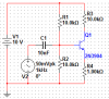
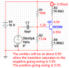
First wouldn't the base voltage for the base of the transistor be something like 5V because of the voltage divider? multisim is reading 2.1V.

Also wouldn't the Ic be 1mA. Multisim is reading 850mA.
 

Attachments

  • CommonEmitterAmp.png
    CommonEmitterAmp.png
    6.1 KB · Views: 401
You bias is not good. R1, R2 wants to pull the base to 5 volts. This should pull the emitter to 5 volts. The gain is set to 10, so the voltage across the collector resistor should go to 50 volts.

You need to change R1, R2. Set the base voltage to about 1.1 volts. The goal is to set C=5 volts, E=0.5 volts, and base to 0.5 + 0.6 volts.
 
Assuming that you think that R2, R3, and R4 should be the values that you have chosen (not the best values, but they will do for now), you would like to choose a value for R1 that biases the collector about halfway between the emitter voltage V(E) and the supply voltage (10V). I used LTSpice as a calculator which plots V(c), V(b), and V(e) as a function of R1. It is also good to check to see what would happen as a function of temperature, too.

Note how LTSpice lets you do both at the same time...

Note that R1=~70K would be good bias point.
 

Attachments

  • DF149.png
    DF149.png
    30.9 KB · Views: 210
Last edited:
Well with the circuit I have posted I need to calculate the base voltage, output voltage, base current, and collector current.
I have made measurement in the lab and got Vc = 1.475, Ic = 0.846mA, Vb = 2.14V, Ib = 0.798mA
 
Do you see that your transistor is saturated? Then it cannot amplify its input signal.
 
Well with the circuit I have posted I need to calculate the base voltage, output voltage, base current, and collector current.
I have made measurement in the lab and got Vc = 1.475, Ic = 0.846mA, Vb = 2.14V, Ib = 0.798mA

Look at the plots I posted. If you extrapolate backwards making R1 less than 40K, what do you see happening?

The '3904 is saturated, and cannot be used as an amplifier. The entire goal of a "bias circuit" is to put the transistor into a condition where its collector is resting at a voltage where the collector can swing both positive and negative, and thus amplify an AC-coupled input. You either missed that point, or chose to ignore it.
 
Is not that I ignored or missed the point. I'm having trouble is with understanding the math that's involved with the circuit I posted. Like by just looking at the circuit, how would I find what Vout should be, what will the base current be, collector current be...etc so I can understand why it's saturated (that's kinda obvious anyways). I know if I used a 100k for R1 and 13.6k for R2 I get Vout to be 5V, which is perfect to swing the AC input.

This is where I'm at right now.

Vb = (R2*10V)/(R2+R1) = 5V
ib = 10V / (R1+R2) = 500uA
ic = ?
Vout = ?
Ve = ?
ie = ?
 
Last edited:
You cannot just put two 10Ks in series, connect the tap to the base of the NPN, and think that the voltage at the tap will be 1/2 of the supply voltage. As both sims have shown you, the tap at the voltage divider is pulled down by what else is connected to it. Note that the voltage across the emitter resistor is (Ib+Ic)*Re. Note that the base (voltage divider tap) is ~0.7V (Vbe) higher than the emitter voltage.

Once Ie is determined, note that Ic is slightly less, and that is what controls the voltage at the collector.
 
I wish that people who use Multisim will turn off the chicken pox dots all over the schematics.

I used a Vbe of 0.65V as shown on a "typical" graph on the datasheet.
The transistor is not biased for a symmetrical signal swing at the output but with your input of only 50mV pk then it is fine.
A load will change it.
 

Attachments

  • transistor.PNG
    transistor.PNG
    9.9 KB · Views: 250
Maybe I'm getting people confused with I'm trying to get or I'm just not interpreting things right.

I understand the transistor is saturated and can't amplify.
What I'm trying to get from this is how all the numbers are obtained. I have attached another schematic from LTSpice. Let's forget about the input AC voltage for a minute. How does the simulation come with all those numbers? What are the calculations done?
 

Attachments

  • Untitled.png
    Untitled.png
    41.7 KB · Views: 155
Are you asking "how does LTSpice work"?

When you direct LTSpice to do a "DC Operating Point" solution (.OP directive), it effectively does a solution of a system of several simultaneous equations in several unknowns until it finds a consistent set of node voltages and branch currents that (hopefully) mimic what the real circuit would do.

If you wrote these same equations yourself, you would hopefully come up with the same node voltages and currents using algebra. If you breadboard this circuit using real parts, hopefully you would be able to measure node voltages that come very close to what LTSpice predicts...

LTSpice is only as good as it's models. Resistors are pretty easy to get right; it is more difficult to get a model of a 2n3904 that works for all temperatures, etc. At that, LTSpice models a typical 2n3904, not necessarily the one you are holding in your hand...

Several posts ago, I showed the real power of LTSpice, which is to answer the broader question: What value of R1 would bias this amplifier so that it would pass a signal without clipping?. Note that what I asked it to do was do hundreds of .OP solutions, varying R1 and temperature, and then plotting the result.
 
Last edited:
Are you asking "how does LTSpice work"?

If you wrote these same equations yourself, you would hopefully come up with the same node voltages and currents using algebra. If you breadboard this circuit using real parts, hopefully you would be able to measure node voltages that come very close to what LTSpice predicts...

What's in bold is what I'm really looking for. I'm trying to find the numbers manually using algebra and with the components given in the circuit (say we didn't have computer).
I built the circuit on a breadboard and the results were pretty close to LTSpice.
 
With the 10k collector resistor, the 1k emitter resistor and a transistor that saturates with its collector to emitter voltage 0.2V then the saturated current is (10V - 0.2V)/(10k + 1k)= x. The saturated voltage at the collector is 10V - (x times 10k ohms).
Also the emitter voltage is x times 1k ohms. So the saturated collector voltage is 1.09V.

The collector voltage when the transistor is cutoff is 10.0V. The average voltage is 5.55V which is where the collector can swing equally positive and negative.

So the collector current is 0.45mA at idle and the emitter current is almost the same so the emitter voltage is 0.45V.
The base voltage must be 0.65V higher at 1.1V.
You can calculate the resistor divider to give 1.1V at the base of the transistor. The very small base current will affect the divider a little.
 
It is nice to be able to design simple circuits, without having to rely on simulators all the time.

Firstly, any bipolar junction transistor, will always need a current flow into the base input to make it work properly.

Be it electron current flow with a PNP, or conventional current flow NPN.

Looking at the circuit it would appear to be half the supply voltage, would be at the center tap of both equal value resistors, which puts it at 5v.

Remove the connection between the transistor base and the voltage divider, and that is the voltage at the tap of the divider. [VCC x R2 /(R1 + R2)] = 5v.

Now with the transistor back in the circuit it drops to 2.13v.

THIS is VERY hard to determine without actually building and taking measurements, unless you know the exact parameters of the transistor being used.

HOWEVER you can learn alot from this circuit, about how a transistor is bilateral meaning, it will effect the input signal, as well as an output.

So lets do an analysis on this circuit, EVEN if this was not a simulator, you still breadboard the circuit, and take all the imperical measurements, to come to a logical analysis of the circuit.

So now these are the measurements you have come up with, (data).

From this data you now can analyse its behavior, AND how to design it so as to eliminate these bad characteristics.

Hopefully you have a good understanding of the basic laws (ohms, kirchoffs,ect...)

Lets start out and determine the loading affect the transistor has on the input voltage.

1. without transistor VR2 = 5v. current IR2 = 500uA.
2. VR1 = 5v. @ 500uA.
3. With transistor VR2 = 2.13v. @ 213uA
4. VR1 will then be (VCC - VR2) = 7.87v. @ 787uA.
5. Delta current through R1 goes from 500uA, to 787uA. = 287uA.
6. Delta IR2 goes from 500uA down to 213uA. = 287uA.
7. If the total current is now 787uA through R1 and 213uA OF IT flows through R2
that leaves (787uA - 213uA) = 574uA. left over to flow into the base of the transistor. = (IB)

That shows how the transistor affects the input signal.

Lets carry the analysis further.

Now a measurement across the emitter resistor determines a voltage of ~ 1.43v. = VR4.

That makes the voltae Vbe = to ( 2.13v. - 1.43v.) = 0.7v.

Now with VR4 measured then the emitter current will be (1.43v. / 1K ohms) = 1.43mA.
Now to solve for collector current we take the emitter current and subtract the base current we calculated earlier.

(1.43mA - 574uA) = 856uA.

From here we can take a quick side note and determine the Beta of this particulatr transistor, at this current value. (B = IC / IB) = ( 856uA / 574uA) = ~1.5

Continuing with the analysis, looks like you took a measurement at the collector as well. = (VC)
so (VC) = 1.44v.....

Hmmmmm if the emitter voltage is at 1.43v. and the collector voltage is at 1.44v. that means a voltage drop of 10mV. is across the transistor = (VCE).

Ok, now you took your measurements and have calculated currents and Beta, ect...
And you have your conclusion, that this design is not a good amplifier.

Now it is at this point where you apply your mathematic calculations, to redesign it so that you can determine the voltages and currents on paper, and get good results in an actual prototype.

Keeping your collector resistor in your design, the same value, you need to rework the value of the base and emitter voltage to get a more workable circuit.

From basic amplifier theory, you know that VC should be around half the supply voltage.
so with VC at 5v. that leaves 5v. to be dropped across the emitter resistor and the transistor.

The collector current is now [(VCC - VC) / R3] = 500uA. = (IC)
Lets use your original 1K ohms for R4. so VR4 will be (500uA. x 1K ohms) = 0.5v.
That puts a nice 4.5v. across the transistor, so it definately is not saturated.

From experiance you know that around 0.7v = Vbe.

So now you can calculate your voltage at the base (VB) so as to turn the transistor on.
(VB) = (VR4 + Vbe) = (0.5v. + 0.7v.) = 1.2v.

NOW a good rule of thumb is, if no input impedance is specified, then it is a good practice to make R2 to be around 10 - 20 times greater than R4. So as to not allow the transistor base current upset the divider, as it did in the previous circuit design.

So lets use your original 10K ohms for R2.
Now with R2 chosen we can now calculate the current through R2, by (VB / R2) = (1.2v. / 10K) = 120uA. = (IR2)

Now to calculate the value of R1 we need this equation. [(VCC - VB) / IR2] = [(10v. - 1.2v.) / 120uA] ~= 73K, so we will use a standard 75K or a 68K ohm resistor.

Now we take the measurements. (AND ADJUST VALUES AS NEEDED)

CEquestion.jpg

So you use your simulator to test out your designs, but get used to calculating first then let your simulator confirm your calcuilations, or point out any errors.

Designing a circuit is as much as prototyping and taking measurements and gathering data, as well as doing the initial calculations.
 
Last edited:
ok, going back to your LTSpice diagram...

let's start with: if the B-E junction is forward biased, Vbe is 0.7V.... period. this is probably what is confusing you the most. a transistor junction is a nonlinear resistance. once you get to a threshold where it starts conducting, it's resistance decreases nonlinearly as the current increases, so the voltage across the junction changes very little as the current increases.

Er1=7.87V, Ir1=787uA
Er2=2.13V, Ir2=213uA
Er3=8.56V,Ir3=856uA
Er4=1.43V, Ir4=1430uA

so the B-E current will be the difference between Ir1 and Ir2, or 574uA, which is also the difference between Ir3 (collector current) and Ir4 (emitter current).

the data sheet says that a 3904 has a beta of 70 at an Ic of 1ma (and we're close to that here), so it would take about 14uA to saturate the transistor in this circuit (ballpark figure), so you can see that you're far beyond saturation here.

so, that's about as simple an analysis and explanation of why the transistor is in saturation as i can come up with...... what somebody said above about setting the voltage divider to more like 1V (without the transistor in circuit) will get you in the ballpark of amplifying a signal rather than saturating the transistor... look again at the Ib(sat) (base current required for saturation) i calculated above and keep that in mind when you select resistor values for the voltage divider.
 
In your 1st circuit it is obvious that the transistor is biased wrongly and is saturated. The emitter resistor value is 1/10th the collector resistor value. We know that the collector voltage should be near half the supply voltage so that the collector voltage can swing equally positive-going and negative-going. The datasheet has a graph that shows the typical base-emitter voltage of 0.65V and we know that the emitter voltage must be 1/10th the collector voltage, about 0.5V. Then we know that the base voltage must be about 1.15V, not 5V.

You can calculate the wrong base voltage because we know the collector and emitter current. The saturated transistor has a collector to emitter voltage of about 0.2V and a supply of 10V. Then the collector and emitter current is (10V - 0.2V)/(10k + 1k)= 0.89mA. The emitter resistor is 1k so the emitter voltage is about 0.89V (but the base current causes the emitter voltage to be a little higher). The base voltage is 0.65V higher at 1.54V, not 5V.
 
Very nice, Thanks all for your help, now I have a better understanding of how the circuit works.

@JCLrd You mentioned that's really hard to determine what the Vb will be after the transistor's base is connected to the tap.
What if I hadn't measured the voltage at the base, how would I be able to find it?
Let's assume I was using this data sheet.
https://www.electro-tech-online.com/custompdfs/2011/02/2N3904-1.pdf

Hello,

If I were to look at your circuit and analyse it, from calculations only, I would do it this way.

I would calculate the voltage divider to be at 5v. (regardless of the base current load)
Then I would subtract an assumed, Vbe, of 0.7v. from that value to give (5v. - 0.7v.) = 4.3v.
Then divide R4 into that voltage to give (4.3v. / 1K) = 4.3mA. = emitter current.
Then multiply that emitter current times R3 which is (4.3mA. x 10K) = 43V. to give the voltage drop across R3.

From there I know that the voltage drop cannot be realized, because its greater than VCC.

So Now I know that the base current has got to be substantial, to load the divider, to cause a great reductionion of base voltage, in order for the voltage drop across R3 to be realized.

Now that was a quick test to see if the circuit is designed properly.
Now I know it is not, I'll do a quick input impedance approximation.

Using thevenins equivalent circuit analysis, I would disconnect the transistor, and soolve for the equivalent resistance and voltage present at the input, base terminal.

This is done as:
Eth = [(VCC x R2) / (R1 + R2)] = [(10v. x 10K) / (10k + 10K)] = 5v.
Rth = [(R1 x R2) / (R1+R2)] = [(10K x 10K) / (10K + 10K)] = 5k

So now you redraw the circuit with a 5v. source in series with a 5K ohm resistor, then this is connected to the base of the transistor.

Now you use the lowest beta value on the data sheet whick is 30 in this case, and you multiply it times R4. which is (Bmin. x R4) = (30 x 1K) = 30K ohms. (first order Aproximation.)

Now you assume a Vbe of 0.7v across the base emitter junction.

Now to solve for the total base current, you take the value of Eth and subtract Vbe, then divide that value by the total series resistance of the calculated emitter resistance of 30K ohms and the Rth value of 5K ohms.

looks like this....[ [(Eth - Vbe) / [(Bmin x R4) + Rth)] ] = [ [(5v. - 0.7v.) / [(30K + 5K)]] = 122uA. = (IB)

Now take that value and multiply it by Bmin. to solve for the collector current, (Bmin x IB) = IC = (30 x 122uA.) = 3.6mA.

Take that value and multiply it by R4 and R3 together to solve for total voltage drop across both resistors.... [(3.6mA x (1K + 10K)] = 40v.

Again unrealizable, so now you have to start changing assumptions, such as Vbe, and Bmin. values, which means a lot of further parameters of the device need to be put into the equations, which gets extremely complicated, for just quick analysis of a circuit, you have to consider every variation of device parameters, ect.....

So to analyse a circuit performance like a computer can do, takes a lot of math and knowledge of device parameters, to get accurate results in the calculations.

The above methods given, are first order appraoximations, to help you analyse a circuit to see if it is a ,go ,or no- go, design, as the above calculations showed it is a ,no-go, design, when used with the Bmin. specified in the data sheet.

That way there you know how to redesign that circuit to give a better result.

Now one other way to analyse a circuit like this would be again to make an assumption, that half the supply voltage is across R3.

That would make a collector current of 500uA.
take that 500uA times R4 and that give an emitter voltage of 0.5v.
Add to that Vbe of 0.7v. and that gives 1.2v. at the base.

So again if the voltage divider is suppose to have 5v. at the tap, and your getting a calculated value of 1.2v, then you know that the voltage divider is being upsetted by the base current, and so the design is a no-go, for an amplifier.

The base current should not control the base voltage, but rather the external voltages by the divider should control the base current.

So thes are quick analysis methods to check if a circuit is designed properly.

As I said before to calculate the way the computer does, means a lot more equations and device parameters need to be used.

Hope this helps...
 
Last edited:
Status
Not open for further replies.

Latest threads

Back
Top