Continue to Site

Welcome to our site!

Electro Tech is an online community (with over 170,000 members) who enjoy talking about and building electronic circuits, projects and gadgets. To participate you need to register. Registration is free. Click here to register now.

  • Welcome to our site! Electro Tech is an online community (with over 170,000 members) who enjoy talking about and building electronic circuits, projects and gadgets. To participate you need to register. Registration is free. Click here to register now.

Can not get common source amplifier working in simulations

Status
Not open for further replies.

Fluffyboii

Active Member
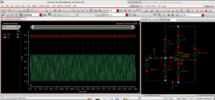
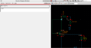
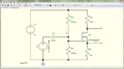
I tried for an hour or so to make a mosfet amplifier in LTspice but I never got gain more than 1 no matter what values I used for bias resistors ,drain resistor, source resistor. If I recall correct gain should be something around -drain resistance/source resistance but nope it just doesn't work.

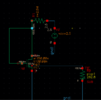
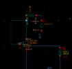
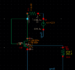
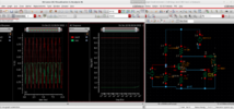
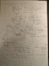
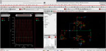
I need to make a amplifier with 8V/V gain with maximum 2.5Vdrain. I will calculate the values with the boring old fashioned way but it seemed odd that I couldn't get anything working with ballpark values. Cadence also had the same issue so I am assuming I forgot something important. (I tried using more Vd in Cadence later, it didn't help)
 

Attachments

  • garbage.asc
    1.4 KB · Views: 221
  • Screenshot_1.png
    Screenshot_1.png
    1.1 MB · Views: 221
Thanks for the insight.

I am not questioning LTC as a simulator, just the notion that one can use
a "generic" MOSFET model, with "generic" parameters, and get better
results than using the manufacturer and device specific ,model. But
that was my misunderstanding from simonbrambles post, #12.

As far as accuracy of LTC, I think of it and the other myriad of simulators as
roughly the same, until proven otherwise. They largely use the same convergence
methods, same analytical choices for engine.....once given the parameters. But
I do not consider myself a sim expert, so would listen to anyone on why one
sim is better than another.

And to point out where model parameters come from, as I helped designers
as a production and test EE at NSC for a few years.

I use simmetrix quite a lot, after using LTC, because probing was so much easier.
I also feel user interface much more friendly. And Analog Devices thought so as
that was their goto sim, until they bought out LTC, and someone made a decision
to settle on LTC, for reasons I do not understand.

For sure LTC, NSC, AD, many great design houses and experts. Used to sit close to
Pease and the linear guys at NSC, as a central apps guy after PE and TE work I did
at beginning of career. The two guys that most impacted me were Gus Mellick,
knew more than god about bipolar transistors, and Barry Siegal who ran the Hybrid
group doing most of the high precision work. Mrazek on 2900 and Carnelli on
interface. Moyer, manager central applications. Very fortunate to have learned from
them. Great times to be in the game, as I am sure are now happening in newer fields.


Regards, Dana.
 
Last edited:
Where is the Gate Bias supplied from here?
In Falstad's sim you can choose a user-slider with variable voltage that shows the applied voltage. I chose a gate voltage interactively. By default, it starts at 0 to 5 but you can edit that range. This is much faster than editing LTSpice. Falstad's is the best tool for level 2 simulation where you add your own discrete parasitics if you want. You can define a dozen characteristics for a diode if you wanted but not have a library. So it is far faster. But LTSpice and TINA are better for Level 3 using specific component models but setup time is greater and feedback is static.
 
I learned how to read schematics from reading (every) EDN design article published in the EE library bound annual volumes and every other resource I could find. So when I started work in '75 it was Aerospace R&D instrumentation with no training except for all the Mil-Std-Handbooks in the library. So my 1st design was a VLF 5 ch. CMOS Doppler Rx. It was installed in the Beaufort Sea on a moving ice flow with a vertical wind turbine a UHF Tx for GOES 1. It was Canada's first floating automated weather station all made by my brilliant mentors at Bristol Aero.


In the late 70's I designed a couple large automated SCADA systems. One for ground rocket launch station using all HP equipment (2 HP9825's ) and programmable power, logic and real-time CRT status display. The other with custom designs of about 40 PCB's , robot and eddy current instruments for probing Candu nuclear tubesheet tubes in an inverted position with XY displays, with 6800 micro control programmed by 2 UofM profs who later went to teach at Waterloo. For example, the MOTOROLA UART had not been released yet so I had to design a PCB for a UART with all the same features with discrete 4xxx logic. For analog I used Burr Brown 12bit ADC/DAC and designed my own 2-way telemetry. everything was MIl-std 883 chips, but ESD awareness was still primitive. Now that was about 45 years ago. Later spent 10 yrs working as TEst Eng Mgr and NPI product mgr from a design from Santa Clara so spent over 10 yrs working in Cali in Disk drive technology. I was offered a senior job (QA Mgr) at Seagate and another in SImi Valley but my (ex) wife designed she didn't like the move from Winterpeg 8)!

I learnt a lot from Japanese designs in the early 80's from the likes of NPL, Hitachi, Toshiba, Fujistu, (all HDD design) and Shindengen power supplies then later Maxtor, Seagate, CDC, Miniscribe, Micropolis etc. . They all had amazing servo designs.

I spent 4 yrs in Telco designing network BER test equipment and managing the network for Project IDA, an ISDN broadband WAN with DS1 (1.544Mbps) FDX to 100 homes in a PRoject IDA trial. in '79.

It was exciting times in EE design during the 70's 80's, later I spent more time in Operations and Management.
 
Last edited:
Let me confirm how Falstad's Sim computes gm when you hover over the FET after you choose Vt & Vgs then choose RdsOn with the link and it computes beta so you can finish the design of a closed loop Common Source amplifier that is almost insensitive to gm and Vt and Vgs if you allow a 10% tolerance in gain reduction from drain loading adding to the Rfb value.

Here I chose a FET much like IRLHS6342 but instead of a switch, used it as linear amplifier. This might be a poor design for other reasons, but it proves how to design an AC control gain in Common Source Amp.

You can do the same in LTSpice to see the frequency response effects of Rfb and Qgs=11nF @1V then decide how to improve by matching Z(f) ratios.

1666368272296.png
.

Take Away

The bottom line here is you cannot make an accurate gain design with an open loop Common Source FET as you can with a Common Emitter with simple gate voltage biasing due to Vth tolerances.

gm is too sensitive to Vgs-Vt and Vt has too wide a tolerance.
Av=−gm*R(Drain)

The reason is for BJT's diodes at 1.0 mA such as Vbe are pretty close to 0.6V for most transistors. Above this current, bulk resistance adds to the voltage rise with significant variation based on power ratings. You can bias Ie and Ve/Re pretty easily from Vb. But FET gate voltage is far more senstive near threshold for Ron and Vth has a typical 2:1 voltage range tolerance.
e.g.
- 2 to 4V for standard FETs or
- 1 to 2.5 for the ON 2N7002 or
- 1.1 to 1.9 for the Toshiba version. T2N7002 ( tighter tolerance on Japanese parts)
- 0.5 to 1.1 for the IRLHS6342 Rds(on) max (vgs = 4.5V) 15.5 mΩ International Rectifier

For giggles how much gain-bandwidth can you get from a closed loop IRLHS6342 in a Common Source Design at 4 mA drain?

But you can simulate the DC and low-frequency characteristics accurately knowing how to use negative feedback. High f (HF) and higher RF demands more experience in geometry and impedance control.
 
Last edited:
Let me confirm how Falstad's Sim computes gm when you hover over the FET after you choose Vt & Vgs then choose RdsOn with the link and it computes beta so you can finish the design of a closed loop Common Source amplifier that is almost insensitive to gm and Vt and Vgs if you allow a 10% tolerance in gain reduction from drain loading adding to the Rfb value.

Here I chose a FET much like IRLHS6342 but instead of a switch, used it as linear amplifier. This might be a poor design for other reasons, but it proves how to design an AC control gain in Common Source Amp.

You can do the same in LTSpice to see the frequency response effects of Rfb and Qgs=11nF @1V then decide how to improve by matching Z(f) ratios.

View attachment 139029.

Take Away

The bottom line here is you cannot make an accurate gain design with an open loop Common Source FET as you can with a Common Emitter with simple gate voltage biasing due to Vth tolerances.

gm is too sensitive to Vgs-Vt and Vt has too wide a tolerance.
Av=−gm*R(Drain)

The reason is for BJT's diodes at 1.0 mA such as Vbe are pretty close to 0.6V for most transistors. Above this current, bulk resistance adds to the voltage rise with significant variation based on power ratings. You can bias Ie and Ve/Re pretty easily from Vb. But FET gate voltage is far more senstive near threshold for Ron and Vth has a typical 2:1 voltage range tolerance.
e.g.
- 2 to 4V for standard FETs or
- 1 to 2.5 for the ON 2N7002 or
- 1.1 to 1.9 for the Toshiba version. T2N7002 ( tighter tolerance on Japanese parts)
- 0.5 to 1.1 for the IRLHS6342 Rds(on) max (vgs = 4.5V) 15.5 mΩ International Rectifier

For giggles how much gain-bandwidth can you get from a closed loop IRLHS6342 in a Common Source Design at 4 mA drain?

But you can simulate the DC and low-frequency characteristics accurately knowing how to use negative feedback. High f (HF) and higher RF demands more experience in geometry and impedance control.
gm I calculated for this mosfet was too low and I think that is why it is impossible to use it for an amplifier. I gave up after working for few hours with no results.
 

Attachments

  • IMG_20221021_013105.jpg
    IMG_20221021_013105.jpg
    859.9 KB · Views: 162
  • Screenshot_2.png
    Screenshot_2.png
    1,001.9 KB · Views: 163
  • Screenshot_3.png
    Screenshot_3.png
    121.1 KB · Views: 168
  • Screenshot_4.png
    Screenshot_4.png
    29.5 KB · Views: 163
  • Screenshot_5.png
    Screenshot_5.png
    29.4 KB · Views: 167
  • Screenshot_6.png
    Screenshot_6.png
    28.6 KB · Views: 161
  • Screenshot_7.png
    Screenshot_7.png
    959.7 KB · Views: 171
gm I calculated for this mosfet was too low and I think that is why it is impossible to use it for an amplifier. I gave up after working for few hours with no results.
The root cause of gm too low was the excess difference of currents with too low a current for Vt which should’ve been 25 µA. Which resulted in over biasing of Vgs. Had you used the bias for that Vt your gm would be much larger. This is the common threshold for high Rdson parts.
You’ll notice by using negative feedback Vgs is only slightly above Vt which allows for greatest gain with a grounded source and also easy self bias.
 
Last edited:
The root cause of gm too low was the excess difference of currents with too low a current for Vt which should’ve been 25 µA. Which resulted in over biasing of Vgs. Had you used the bias for that Vt your gm would be much larger. This is the common threshold for high Rdson parts.
You’ll notice by using negative feedback Vgs is only slightly above Vt which allows for greatest gain with a grounded source and also easy self bias.
I see. I tried different bias voltages later with no luck after that while keeping Rd 10k and Rs 1k with no luck. I also got rid of bias resistors and tried adding DC offset from the AC source itself to try like 700mV but nope nothing worked. I never got more than 1 times gain. I don't know how to use feedback on transistor amplifiers but I guess I will find that out in the next analog circuit design lecture.

It looks like for 25nA Vt is 0.783V
 
Last edited:
I don't know how to use feedback on transistor amplifiers but I guess I will find that out in the next analog circuit design lecture.

The basic concept is very simple, for the type of circuit you started with.

Think of the transistor (Bipolar or FET ) as a source follower / emitter follower:

The voltage across the source or emitter resistor will vary (almost) the same as the gate / base voltage varies.
(Assuming everything stays in practical limits.)

I'll stop using both device type designations & stick with bipolar, though it still applies to both.


So, the current in the emitter resistor will vary in proportion to the source voltage. It work as a voltage controlled current source (or sink), with the current controlled by the base voltage.

That same current, or nearly so, passes through the collector. That means the voltage across the collector load is also, indirectly, proportional to the base voltage & emitter current.

If the collector resistor is equal to the emitter resistor, the voltage changes will be the same, but inverse, the collector voltage reducing as the emitter voltage increases.

If the collector resistor is eg. 10x higher value, you get 10x the voltage across it as on the emitter - and 10x the voltage change as on the emitter. The emitter is following the base, so 10x voltage gain base to collector.

Adding a resistor and capacitor across the emitter resistor increases the AC signal gain without affecting the DC bias calculations, so you can get high gains without excessively high ratios of collector to emitter resistance that make DC biasing difficult.


You just have to set the resistor values for sensible current for the transistor in use and the application, and set the base bias voltage appropriately to set the emitter and therefore collector voltages to allow a good voltage variation in both positive and negative swing; eg. collector probably somewhere between half and 2/3 supply, depending on gain etc.

That's partly from looking as the device data and partly experience.

[Neither bipolar or FET devices exactly follow the ideal emitter follower / source follower voltages, due mainly to the base current passing through the emitter resistor with a bipolar transistor, and the gate-source voltage varying with source-drain current with a FET - but the concept and basic principles above apply].
I understand this but I don't know how to design multiple transistor amplifiers that are more stable and causes less distortion of the input signal. For this time I was trying to make a single simple amplifier like you described yet it refused to work in Cadence. I will personally ask the teacher why.
 
Another way of thinking the same thing.

How does gm compare with 1 / Ron ??

- Max gain is achieved by utilizing this impedance ratio concept and appropriate loading values and Vgs bias.


The common drain circuit has some good functions but also disadvantages with bias sensitivity and offset DC voltage which can be corrected with more complex configurations.

- Differential mode, constant current bias

Regarding your Cadence last photo.:
The 1K load was too small a value for the output impedance of the circuit by loading and DC coupled affected Vgs biasing below threshold so impedance ratios prevented any gain

Try this link or in Cadence Beta = 2, Vth= 1.5


1666533258735.png


Change Values with mouse wheel in Falstad or create slider
1666534058959.png


When designing analog FETs with high gain use large W/L ratio up to 1200 or so depending on noise effects.

The 1A Falstad example was ridiculous but head-bangs the point that high impedance ratios AC coupled allows for great voltage gain but at the loss in impedance buffer gain of out/in


Review Theory here


You will find the forward conductance gm in the IRFL014 rated in Siemens is high since Rdson is low as a switch. which I approximated in Falstad sim with beta = 2 but left Vt= 1.5 rather than some value between 2 to 4V
1666534849583.png
 
Last edited:
I am leaving this here. I was able to learn using Cadence better while writings this so it is quite messy and problematic report if it can be called that. But I was able to get some stuff working even though my hand calculations always failed me. I will post the layout stuff when its due date is over. I am trying to understand small signal calculations with added second characteristic effects like ro and body effect but it gets quite complicated very quick.

It turns out thermal voltage is all over the place and it keeps making hand calculations useless. Also cut off region gives more gain due to its exponential nature. It is so imperfect that it drives me mad.

I also thought Width of the mosfet would affect gate capacitance and ruin the bandwidth in case it is too much but it turns out it doesn't really effect 3dB point in simulation. Maybe all though put into it is in vain idk.
 

Attachments

  • CS amplifier in Cadence.pdf
    3.3 MB · Views: 338
1668356714663.png
Sorry, I thought you were looking for a better circuit design, not a level 6 FET parameter design.

You might want to modify your schematics to be more readable and eliminate dots and use the same color background as your document or a neutral or pastel shades.

vs hard to read this
1668356380184.png


- also avoid jagged lines and loops and reduce blank space or group in logical ways , this is a SAW osc.
1668360396291.png


In your FET simulations, you should find that Ciss * RdsOn or Coss * RdsOn result in a relatively constant FOM's that is evident with many families of FETs. But there are ways to reduce this and extend bandwidth but at the tradeoff of other parameters with voltage and power ratings and other 3D parameters.
 

Attachments

  • 1668356976598.png
    1668356976598.png
    136.8 KB · Views: 155
Last edited:
View attachment 139269Sorry, I thought you were looking for a better circuit design, not a level 6 FET parameter design.

You might want to modify your schematics to be more readable and eliminate dots and use the same color background as your document or a neutral or pastel shades.

vs hard to read this
View attachment 139268

- also avoid jagged lines and loops and reduce blank space or group in logical ways , this is a SAW osc.View attachment 139275
Is that a saw oscillator. I didn't know you could do something without diode and just 4 bjts.
I can name the lines for better understand ability of the circuit as you said but I was a bit lazy and it doesn't make it harder to understand for me but I get the reason why it is not ideal. Level 6 must be very complex I guess I can not really predicts its behaviors without good intuition.

I don't know how to change the background and such in Cadence though, it is a program with a very outdated user interface.
 
Here's an update of your original ltspice circuit, set up as I described.
Note that the original did not have any connection between the bias resistors and gate!
(The mosfet is just a small signal one I picked at random from the available parts).

FET_Amp.png
 

Attachments

  • FET_Amp.asc
    1.6 KB · Views: 150
Here's an update of your original ltspice circuit, set up as I described.
Note that the original did not have any connection between the bias resistors and gate!
(The mosfet is just a small signal one I picked at random from the available parts).

View attachment 139276
Yes my original circuit was garbage because I forgot to connect the bias to gate. The thing with mosfets in Cadence is that their output resistance is low and it is pulling the Rd to a lower value since they are parallel -gmRd becomes -gm(Rd // ro). And bias voltage gets hard to decide because Vt changes with Id. Increasing the Width of the mosfet increases Id and gm but after some point it loses its effect. Because all variables are tangled to each other I can not apply the normal mosfet knowledge I got at advanced electronics class in analog design class. LTSpice simulation just doesn't cut it at that level. Also body effect decreases the effective resistance of the diode connected mosfet and decreasing its equivalent resistance. When I should get 22 times gain I get like 6-10. Considering all that and adjusting the values is to difficult.
 
You appear to have the source grounded in the Cadence circuit (though it's difficult to make out).
You must have a source resistor to stabilise the bias and device current.

I don't have cadence so I cannot do anything with that circuit.
 
You appear to have the source grounded in the Cadence circuit (though it's difficult to make out).
You must have a source resistor to stabilise the bias and device current.

I don't have cadence so I cannot do anything with that circuit.
Yes I Rs would make it more linear and stop gain from being dependent on gm but teacher asked for 10 gain which was impossible to have with source resistance since it decreases gain.
 
so would listen to anyone on why one
sim is better than another.
All Spice based simulators are likely quit similar in their accuracy but, I think Falstad uses a different and simpler simulation engine, so I would not expect it to be as accurate.
 
Last edited:
Status
Not open for further replies.

Latest threads

New Articles From Microcontroller Tips

Back
Top