This question is a good example of how a simple question gets lots of interesting info but doesn't seem to hit the mark.
Cannot get common source amplifier working in simulations
This is a simple DC question that is about gm, or it's inverse RdsOn and the factors that control gain, including Rs, Rd and Vdd.
In this case it has nothing to do with frequency response or gate charge or Miller Capacitance at DC. You should understand already that diode
capacitance increases with rated current which means with
lower bulk resistance junctions. The same is true for MOSFET DS junctions. Thus the RC =Time contant is relatively fixed for any given family of FETs with variations in conductor and semiconductor gaps but changes with vendor process and 3D design.
So don't mind C, Q, f, and LTSpice models for now. Let's go to basics for DC gain.
RdsOn is static resistance of drain to source as a switch at fixed Vgs voltage, but for an analog amplifier we need to know the sensitivity of output current/voltage that causes gain, which is the factor
gm which is the inverse of the dynamic drain-source resistance, let's call it
Ron.
Adding the source Rs reduces gain since it adds to R
on and reduces the sensitivity of Vgs as the input control voltage.
- The
threshold of Vgs where R
on starts to change rapidly and conduct is either called
Vgs(th) or abbreviated to
Vth or Vt (depends if the company is Japanese or American or German etc). Recall also in the EU, voltage V = U for equivalent use.
for the Toshiba 2N7002
For onsemi 2N7002
- It is low constant drain current with Vds=Vgs ( gate to drain short)
- It is just the threshold ! and not enough to be used as an analog amp. or a switch.
So remember that to use a FET switch, Vdd must be at least 2 to 3x this Vt threshold.
- High R
on devices might specify 50 uA for Vt or low R
on devices at 250 uA
Let's cut to the chase
So the only
critical factors for analog gain in choosing an Enhancement-Mode FET (Nch or Pch) are
RdsOn and
Vgs(th)=Vt
In the saturation region,
Ids = beta * (Vgs - Vt)²/2. (This is not the same beta=hFE used in bipolar junction transistors (BJT) like NPN type for current gain.)
CMOS just uses both polarities of FETS (Nch & Pch) Each generation is lower Vt and lower Rds(on) and is generally all the same for all suppliers but
beta has a wide tolerance +/-50% , some mfg. later reduced to +/-33%.
Using a model typical for
CMOS used in all CD4xxx series logic which is good for high gate voltage range and Vdd but also high Ron values they used
Vt=1.5V and beta=50m (circa 1970) for the CD4xxx family (based on my experience only)
The simulation link demonstrates how Vt is measured
beta=50m using a simple Nch model with 25 uA.
Think of the threshold Vt as a very low voltage constant voltage Zener but with a very high resistance (knee threshold) so resulting Vt is constant.
That is the same as 60k resistor.
If Id is raised to 250 uA the same FET Vt=1.60 V which is now equivalent to
Rds=6.4kΩ, gm= 5 mA/V
This current gain is all due to the quadratic effect above threshold. (
Ids = beta * (Vgs - Vt)²/2 )
Simple Design Analysis
So to make it more linear you add a source resistor Rs but made it far too big for the current Id.
Whereas in my
previous design suggestion #14 I shorted the source resistor, and both Pch & Nch with negative feedback R Ratios to
reduce the gain, reduce the output impedance and significantly reduce harmonic distortion for large swings.
Simple design for a common source.
- consider 250 uA average drain = Id
- for beta = 50m gm = 5mA/V Ron = 6.4k @ 250 uA
- consider 20 % of Vt for source resistor drop
- 250uA*1k = 250 mV , Let Rs=1k if Rd = 10*Rs then it would have a DC drop of 2.5V from Vdd.
- Let's consider Rs = twice what Ron was at 250uA for the Threshold voltage. thats Rs=2x6.4k= 12.8k
- now to bias the gate at 1.6V to get Id average = 250 uA we need to add 250 mV source DC to bias the gate now at 1.85V .
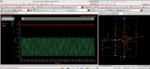
- so I simulated it with an adjustable V source and 1M series resistor, you can make any voltage divider to do the same. Then I AC couple a signal with 1Vpp input.
- guess what ?
- the output gain is near what you wanted = 8x
I could have done a rigorous mathematical design solution but here I wanted to use a minimum of math and show an interactive method to find gain and use the simplest physics model used in Falstad's based on Vgs, Vt to get Ron, and gm then choose Vg then Rs and Rd.
Any questions?
Now realize that this design is not as accurate as a BJT due to the wide tolerances on Vt and this "open-loop" style of bias. So raising Vg will increase the current and gain rapidly and real devices will have a wide tolerance so unless you use a regulated current or negative feedback,
this design is not very commonly used.
upon zooming in the output was clipping at 12V and the gain was actually 10.6, after I reduced the input to 100mV pp.
design of low gain common source linear single Nch Enh-mode FET amplifier.
Gain =10 approx.


