philba
New Member
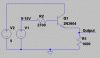
I have been looking at the common collector configuration of an NPN transistor and can't fiugre out why it works the way it does. I've not found anything online that helps me understand this. Horowitz/Hill only has a brief section on it.
By the way, the CC config looks like a nice way to reduce input voltage with out dividing it and thus increasing impedence. Of couse, you have to deal with Vbesat drop.
So, my main question is why is the output voltage at the emitter limited to the base voltage (minus Vbesat). What is the mechanism? Maybe a better way to ask it is why is the voltage gain approximately 1 (actually (Vb - Vbesat)/Vb )?