Continue to Site

Welcome to our site!

Electro Tech is an online community (with over 170,000 members) who enjoy talking about and building electronic circuits, projects and gadgets. To participate you need to register. Registration is free. Click here to register now.

  • Welcome to our site! Electro Tech is an online community (with over 170,000 members) who enjoy talking about and building electronic circuits, projects and gadgets. To participate you need to register. Registration is free. Click here to register now.

Can not get common source amplifier working in simulations

Status
Not open for further replies.

Fluffyboii

Active Member
I tried for an hour or so to make a mosfet amplifier in LTspice but I never got gain more than 1 no matter what values I used for bias resistors ,drain resistor, source resistor. If I recall correct gain should be something around -drain resistance/source resistance but nope it just doesn't work.

I need to make a amplifier with 8V/V gain with maximum 2.5Vdrain. I will calculate the values with the boring old fashioned way but it seemed odd that I couldn't get anything working with ballpark values. Cadence also had the same issue so I am assuming I forgot something important. (I tried using more Vd in Cadence later, it didn't help)
 

Attachments

  • garbage.asc
    1.4 KB · Views: 223
  • Screenshot_1.png
    Screenshot_1.png
    1.1 MB · Views: 223
Changes:
No connection R3,4 & C1,M1. No bias for M1.
Change 2m to 2Meg. 0.002 ohms to 2,000,000 ohms.
R5 load 300 ohms is too low. The R1 10k cannot drive a 300 ohm load.
I have had trouble with the mosfet you choose. I changed to a real part.
View attachment 138979
Isn't "m" and "Meg" stand for the same thing. I tried with load and no load but it makes sense if writing "m" doesn't stand for mega ohm in LTSpice.
 
.. and it is always better to use one of the FETs internal to LTspice. These are simplified, so run much quicker than FETs downloaded from external sites

I think it would be prudent, where ever possible, to use the manufacturers spice
model, to get accurate results, given the wide variation in device to device variation,
like parasitic C, threshold, drain capability.

Unless of course you modify the generic model to reflect correct spice parameters..


Regards, Dana.
 
.. and it is always better to use one of the FETs internal to LTspice.
The default FET model normally needs its parameters edited for it to be of much use.
 
Isn't "m" and "Meg" stand for the same thing.
Lowercase m always stands for milli, never mega (otherwise what you you use for milli?)
So, for example, mHz is milliHertz, not megaHertz (I've seen many posters make that error on these sites)
Normally, capital M would stand for mega, but since LTspice does not recognize the difference between upper and lower case letters, M also stands for milli, so it uses meg or MEG for mega.
All right, I got it working this time with the danadak's changes. I can't believe totally forgot that stuff in a month or so.
 
I think it would be prudent, where ever possible, to use the manufacturers spice
model, to get accurate results, given the wide variation in device to device variation,
like parasitic C, threshold, drain capability.

Unless of course you modify the generic model to reflect correct spice parameters..


Regards, Dana.
Since LTspice was originally designed for dc/dc converter simulation, its FETs are accurately modelled for input QG and RDSON. Other parameters may deviate from the datasheet spec.

Your comment above assumes that the manufacturer's model is correct and this is not always (rarely) the case. Also, if you use a manufacturer's model, often the circuit will simulate very well until that first rising edge on the gate, then everything slows down as LTspice processes the model. If you are prepared to wait, then please use the manufacturer's model. It will be slower and possibly not accurate.
 
Since LTspice was originally designed for dc/dc converter simulation, its FETs are accurately modelled for input QG and RDSON. Other parameters may deviate from the datasheet spec.

With thousands of MOSFET variants how possibly can one generic model accurately
sim gate charge, capacitance variations from one to another. Let alone HV versus
logic level vs, process variations, technology variations vertical vs planar......
That's sheer nonsense. Why does LTspice have several manufacturers databases of
models and allow import of models ? Because of these variations.

That's like saying LTSpice has one resistor model that covers all resistor values
with magic anticipation of the circuit its been placed in.

Your comment above assumes that the manufacturer's model is correct and this is not always (rarely) the case.

Totally agree, they do not even cover gravitational effects from nearby black holes on channel
conduction. But they do seem to have reasonable, for the most part, predictive circuit behaviour
in sims. Are they exact ? No, nor is the physics of the universe, but we do know how to roughly
model orbit behavior, even though we exclude all the galaxy's mass from the edge of the
universe, most of the universe, in those models.

No model is totally exact, but many seem to be adequate. Process parameters used in them,
I know because I regularly reported that as characterization data to design teams. Used for
their design models.


Regards, Dana.
 
Last edited:
The complementary approach works better with more gain and lower output impedance. Here I used a Beta of 50m which is a fairly high RdsOn FET with Vt=1.5V https://tinyurl.com/2fd55zd9

Without a load of 1k, the gain will be slightly less than the feedback R Ratio here 330k/22k =15

1666106364949.png


With more current and gain I could get around Av= -1500 with no load and R ratio of 5k
Of course the cross-conduction current may be reduced with more complexity.
 
With thousands of MOSFET variants how possibly can one generic model accurately
sim gate charge, capacitance variations from one to another
Thank you for your interesting viewpoint. If you look closely, LTspice has a library of MOSFET models. Click on the AND gate symbol, navigate to "nmos", place the component on the schematic. Then right click over the NFET, select Pick New MOSFET. A magical list appears of the all the different MOSFETs and each one of these should be accurately modelled for input QG and RDSON.

You can do the same with capacitors and inductors. LTspice has a library of these parts, accurately modelled.

This is the point I was making that you misunderstood.

If you want to use a 3rd party MOSFET, you can do. All I am saying is that it might not be accurate and it will probably be slow. You are better picking a MOSFET from the library of parts that has a similar QG and RDSON and simulating with that part. It will run quicker and give results that are 99% accurate - at least for a dc/dc converter

I hope that explains my viewpoint. If you need further clarification, please let me know. I am sure you will
 
So I went into their model library to see how much more exact their models
are, picked at random a 6342, got this :

.model IRLHS6342 VDMOS(Rg=2.1 Vto=0.95 Rd=7.25m Rs=0.0m Rb=4m Kp=60 Cgdmax=2.0n Cgdmin=20p Cgs=0.25n Cjo=0.15n Is=220p ksubthres=.1 mfg=International_Rectifier Vds=30 Ron=12m Qg=11n)

Here are the parameters allowed by spice for a MOSFET :


As you can see LTC is using a subset just like, I would posit, the rest of the
simulators.

So my question is, where did you hear that LTC is much more accurate, source ?
I will correct myself if I am wrong, thats called professional engineering. Would
not be the first time I had junk in my head :)

If you need further clarification, please let me know. I am sure you will

Regards, Dana.
 
Last edited:
This question is a good example of how a simple question gets lots of interesting info but doesn't seem to hit the mark.

Cannot get common source amplifier working in simulations​

This is a simple DC question that is about gm, or it's inverse RdsOn and the factors that control gain, including Rs, Rd and Vdd.

In this case it has nothing to do with frequency response or gate charge or Miller Capacitance at DC. You should understand already that diode capacitance increases with rated current which means with lower bulk resistance junctions. The same is true for MOSFET DS junctions. Thus the RC =Time contant is relatively fixed for any given family of FETs with variations in conductor and semiconductor gaps but changes with vendor process and 3D design.

So don't mind C, Q, f, and LTSpice models for now. Let's go to basics for DC gain.

RdsOn is static resistance of drain to source as a switch at fixed Vgs voltage, but for an analog amplifier we need to know the sensitivity of output current/voltage that causes gain, which is the factor gm which is the inverse of the dynamic drain-source resistance, let's call it Ron.

Adding the source Rs reduces gain since it adds to Ron and reduces the sensitivity of Vgs as the input control voltage.

- The threshold of Vgs where Ron starts to change rapidly and conduct is either called Vgs(th) or abbreviated to Vth or Vt (depends if the company is Japanese or American or German etc). Recall also in the EU, voltage V = U for equivalent use.

for the Toshiba 2N7002
1666200904310.png

For onsemi 2N7002
1666201086947.png

- It is low constant drain current with Vds=Vgs ( gate to drain short)
- It is just the threshold ! and not enough to be used as an analog amp. or a switch. So remember that to use a FET switch, Vdd must be at least 2 to 3x this Vt threshold.
- High Ron devices might specify 50 uA for Vt or low Ron devices at 250 uA

Let's cut to the chase

So the only critical factors for analog gain in choosing an Enhancement-Mode FET (Nch or Pch) are RdsOn and Vgs(th)=Vt

In the saturation region, Ids = beta * (Vgs - Vt)²/2. (This is not the same beta=hFE used in bipolar junction transistors (BJT) like NPN type for current gain.)

CMOS just uses both polarities of FETS (Nch & Pch) Each generation is lower Vt and lower Rds(on) and is generally all the same for all suppliers but beta has a wide tolerance +/-50% , some mfg. later reduced to +/-33%.

Using a model typical for CMOS used in all CD4xxx series logic which is good for high gate voltage range and Vdd but also high Ron values they used Vt=1.5V and beta=50m (circa 1970) for the CD4xxx family (based on my experience only) The simulation link demonstrates how Vt is measured
beta=50m using a simple Nch model with 25 uA.

Think of the threshold Vt as a very low voltage constant voltage Zener but with a very high resistance (knee threshold) so resulting Vt is constant.

1666201642169.png


That is the same as 60k resistor.
1666201885208.png

1666201981675.png


If Id is raised to 250 uA the same FET Vt=1.60 V which is now equivalent to Rds=6.4kΩ, gm= 5 mA/V

This current gain is all due to the quadratic effect above threshold. ( Ids = beta * (Vgs - Vt)²/2 )

Simple Design Analysis
So to make it more linear you add a source resistor Rs but made it far too big for the current Id.

Whereas in my previous design suggestion #14 I shorted the source resistor, and both Pch & Nch with negative feedback R Ratios to reduce the gain, reduce the output impedance and significantly reduce harmonic distortion for large swings.

Simple design for a common source.
- consider 250 uA average drain = Id
- for beta = 50m gm = 5mA/V Ron = 6.4k @ 250 uA
- consider 20 % of Vt for source resistor drop
- 250uA*1k = 250 mV , Let Rs=1k if Rd = 10*Rs then it would have a DC drop of 2.5V from Vdd.
- Let's consider Rs = twice what Ron was at 250uA for the Threshold voltage. thats Rs=2x6.4k= 12.8k
- now to bias the gate at 1.6V to get Id average = 250 uA we need to add 250 mV source DC to bias the gate now at 1.85V .
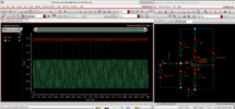
- so I simulated it with an adjustable V source and 1M series resistor, you can make any voltage divider to do the same. Then I AC couple a signal with 1Vpp input.
- guess what ?

- the output gain is near what you wanted = 8x

I could have done a rigorous mathematical design solution but here I wanted to use a minimum of math and show an interactive method to find gain and use the simplest physics model used in Falstad's based on Vgs, Vt to get Ron, and gm then choose Vg then Rs and Rd.

Any questions?

1666204728492.png


Now realize that this design is not as accurate as a BJT due to the wide tolerances on Vt and this "open-loop" style of bias. So raising Vg will increase the current and gain rapidly and real devices will have a wide tolerance so unless you use a regulated current or negative feedback, this design is not very commonly used.

upon zooming in the output was clipping at 12V and the gain was actually 10.6, after I reduced the input to 100mV pp.


design of low gain common source linear single Nch Enh-mode FET amplifier.
Gain =10 approx.

1666205494690.png
 
Last edited:
This question is a good example of how a simple question gets lots of interesting info but doesn't seem to hit the mark.

Cannot get common source amplifier working in simulations​

This is a simple DC question that is about gm, or it's inverse RdsOn and the factors that control gain, including Rs, Rd and Vdd.

In this case it has nothing to do with frequency response or gate charge or Miller Capacitance at DC. You should understand already that diode capacitance increases with rated current which means with lower bulk resistance junctions. The same is true for MOSFET DS junctions. Thus the RC =Time contant is relatively fixed for any given family of FETs with variations in conductor and semiconductor gaps but changes with vendor process and 3D design.

So don't mind C, Q, f, and LTSpice models for now. Let's go to basics for DC gain.

RdsOn is static resistance of drain to source as a switch at fixed Vgs voltage, but for an analog amplifier we need to know the sensitivity of output current/voltage that causes gain, which is the factor gm which is the inverse of the dynamic drain-source resistance, let's call it Ron.

Adding the source Rs reduces gain since it adds to Ron and reduces the sensitivity of Vgs as the input control voltage.

- The threshold of Vgs where Ron starts to change rapidly and conduct is either called Vgs(th) or abbreviated to Vth or Vt (depends if the company is Japanese or American or German etc). Recall also in the EU, voltage V = U for equivalent use.

for the Toshiba 2N7002
View attachment 139002

For onsemi 2N7002
View attachment 139003
- It is low constant drain current with Vds=Vgs ( gate to drain short)
- It is just the threshold ! and not enough to be used as an analog amp. or a switch. So remember that to use a FET switch, Vdd must be at least 2 to 3x this Vt threshold.
- High Ron devices might specify 50 uA for Vt or low Ron devices at 250 uA

Let's cut to the chase

So the only critical factors for analog gain in choosing an Enhancement-Mode FET (Nch or Pch) are RdsOn and Vgs(th)=Vt

In the saturation region, Ids = beta * (Vgs - Vt)²/2. (This is not the same beta=hFE used in bipolar junction transistors (BJT) like NPN type for current gain.)

CMOS just uses both polarities of FETS (Nch & Pch) Each generation is lower Vt and lower Rds(on) and is generally all the same for all suppliers but beta has a wide tolerance +/-50% , some mfg. later reduced to +/-33%.

Using a model typical for CMOS used in all CD4xxx series logic which is good for high gate voltage range and Vdd but also high Ron values they used Vt=1.5V and beta=50m (circa 1970) for the CD4xxx family (based on my experience only) The simulation link demonstrates how Vt is measured
beta=50m using a simple Nch model with 25 uA.

Think of the threshold Vt as a very low voltage constant voltage Zener but with a very high resistance (knee threshold) so resulting Vt is constant.

View attachment 139004


That is the same as 60k resistor.
View attachment 139005
View attachment 139006

If Id is raised to 250 uA the same FET Vt=1.60 V which is now equivalent to Rds=6.4kΩ, gm= 5 mA/V

This current gain is all due to the quadratic effect above threshold. ( Ids = beta * (Vgs - Vt)²/2 )
The beta in current formula is Cox*u*(W/L). In my textbook it says that gm is k(Vgs-Vt) ("k" must be same with beta.) and it also says gm=(delta id)/(delta Vgs). For someone below average like me it really sucks when all textbooks use different symbols for variables so I stick with my old textbook instead for notations.

I struggled for a while to understand how you calculated the gm.
In your test setup Vgs and Vds are same because gate and drain are connected to each other so I should get gm when I follow the "delta id/delta Vgs" (or whatever the triangle represents here, I really hate the triangle)
1666253884958.png


(I assumed that means the ratio of change in those two values so (250x10^-6 - 25x10^-6)/(1.6-1.5) but that doesn't give 5mA/V But using 2id/Vgs-Vt formula from the book gives it. I never thought what gm really was and just memorized formulas so that is what I get as a result.
Is the purpose of using 25uA for seeing the Vt instead of calculating the gm. Can you elaborate on it bit more on how can I calculate these values for a mosfet with it's values unknown.

But there is also channel length modulation calculated in simulation so the value would change if you use something else than 250uA. I think I am supposed to calculate that as well. I guess best way for that would be measuring it with different Id values and getting it from the Id equation with channel length modulation added. (1+λ).

The problem is in Cadence I only have W: 150n and L: 130n for Mosfet model and no oxide capacitance or electron mobility n or λ or L_effective and other details like multiple capacitances inside the mosfet that effect the bandwidth. Teacher didn't specify how detailed we should calculate and just wanted a amplifier with 8 gain and show the -3db point. I mail him for more details.

We simulated a circuit in lab very similar your circuit in the lab class yesterday. Bias is 600mV set within the AC source. This is probably the kind of circuit teacher doesn't expect from students with a not graded assignment but wants to see. I think the PMOS on top here is being used like the resistor Rd checking the textbook so it probably still the same CS setup at the end with no Rs. But I guess that is how it is implemented irl.

The bottom was the circuit I came up with after just blindly trying the stuff from LTSpice in Cadence and the one under it is the Lab example. I want to design it logically like you did with more detail tbh but I really lack the intuition and knowledge to do so which is frustrating.
1666253372256.png
1666251733032.png
 
Last edited:
The complementary approach works better with more gain and lower output impedance. Here I used a Beta of 50m which is a fairly high RdsOn FET with Vt=1.5V https://tinyurl.com/2fd55zd9

Without a load of 1k, the gain will be slightly less than the feedback R Ratio here 330k/22k =15

View attachment 138994


With more current and gain I could get around Av= -1500 with no load and R ratio of 5k
Of course the cross-conduction current may be reduced with more complexity.
Where is the Gate Bias supplied from here?
 
Hello danadak

OK, seeing as you asked….

Firstly, in the words of the Rolling Stones, please allow me to introduce myself..

I worked for Maxim for 10 years as an analogue circuit designer. I then worked for Linear Technology who wrote LTspice. How did I learn LTspice? By getting drunk with Mike Engelhardt, the author of LTspice and spending hours in the car with him. Indeed if you look in the Help files of LTspice, my website is referenced: Help -> Contents Tab -> FAQ -> Additional Resources.

Now, Silicon Valley is known as being the centre of excellence for the world’s electronics industry and, within Silicon Valley Linear Technology is known as the Home of the Gurus. So I have worked quite extensively with the world’s finest minds in analogue circuit design. I still get things wrong, but that is my background.

Back to FETs…

Attached is the circuit I have been playing with, using the FET you suggested
Picture1.png


The Gate-Source turn on voltage is specified as 0.5V – 1.1V

Run the simulation and probe the gate-source voltage at the point where the drain current is 10uA. I get 595mV which is a close approximation to the datasheet spec
Picture2.png


I then probed the drain voltage and drain current. We see that the drain current rises to its maximum before the drain voltage starts to fall. This is how FETs *really* work and the drain voltage and currents don’t cross at the midway point as some text books suggest
Picture3.png


We can also see the Miller plateau in the gate waveform. This Miller plateau is at 1.488V which again adheres to the datasheet graph

Now to measuring input charge:

Probe the current in R1. If the current probe is pointing towards V1, you can hit the <F7> key and turn around the resistor so the current, when probed, flows in the other direction. This gives the instantaneous current flowing in R1. To get the charge, we know that

Charge = Amps x time

So if we integrate the current waveform with respect to time, we can get the total charge. I set up a behavioural voltage source that outputs a voltage equivalent to the integral of the current. I got the following plots:

Picture4.png


If we move the cursors to the far right of the screen, where the VGS has increased to the 4.5V level (as specified in the datasheet), we can see that the total charge is 12.65nC. The datasheet states 11nC typical

If we set up differential cursors and zoom in to the Miller region, we can see the gate-drain charge (Qgd) is 4.6nC, exactly the spec in the datasheet:
Picture5.png


If we zoom right into the initial rise time of the gate waveform, before the Miller plateau, we can see the Qgs at 500pC, exactly the spec in the datasheet:

Picture6.png


Now to measure the ON resistance:

At 4.5V gate-source voltage, the drain source voltage is 101.79mV:
Picture7.png


The drain current is 8.5A, so the ON resistance of the FET is 11.9mOhms. The datasheet states 11mOhms at this gate drive voltage.

So the results look pretty good to me.

So, as I said above, LTspice does accurately model input QG and RDSON and the internal library of FETs are simplified to allow the simulation to run faster, but not in such a way that the accuracy of the simulation is compromised.

I hope the above helps

Simon Bramble
 

Attachments

  • Draft1.asc
    1.3 KB · Views: 177
Status
Not open for further replies.

Latest threads

New Articles From Microcontroller Tips

Back
Top