Continue to Site

Welcome to our site!

Electro Tech is an online community (with over 170,000 members) who enjoy talking about and building electronic circuits, projects and gadgets. To participate you need to register. Registration is free. Click here to register now.

  • Welcome to our site! Electro Tech is an online community (with over 170,000 members) who enjoy talking about and building electronic circuits, projects and gadgets. To participate you need to register. Registration is free. Click here to register now.

Can anyone explain this?

Status
Not open for further replies.

Pommie

Well-Known Member
Most Helpful Member
I have a pic project that I was attempting to add a TM1637. It wan't working and I ended up putting the scope on the clock and data lines. The clock line had additional clocks than it should have had. As I had various other bits of code and after much head scratching, I started a new project with just the following code,
Code:
#include <xc.h>
#include <stdint.h>

#define _XTAL_FREQ 32000000

void main(void){
    ANSELB=0;
    OSCCON1 = 0x60;     //HF int osc
    OSCFRQ = 0x07;      //32MHz clock
    BORCON = 0x00;
    LATB4=1;
    TRISB4=0;
    LATB4=0;
    __delay_us(250);
    LATB4=1;
    while(1);
}
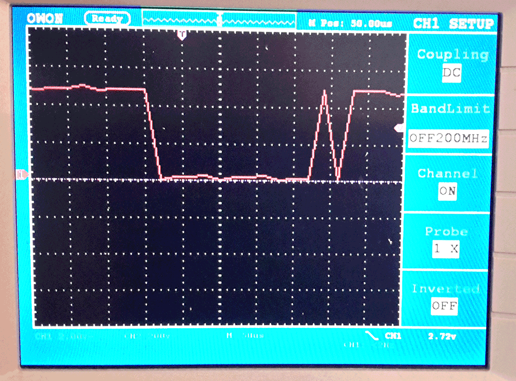
This is what I see on the scope.
scope1.png

The timebase is 50uS.
If the delay is shorted to 50uS I see this,
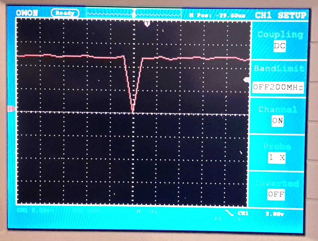
scope2.png

I started with a 16F18346 and then changed to a 16F18446 but it made no difference.
I've powered it from PK4 and a separate power supply - no difference.
WDT is off.

The scope has a 1kHz output which it shows as a perfect square wave.

Anyone any ideas what might cause this?
I'm hoping I've done something really stupid so I can get on with this.

Mike.
 
Why are you setting LATB4=1 before setting it to an output?
It ensures that the output stays high and doesn't trigger the scope. I've got a 10k pullup on the pin. Forgot to mention, tried C0,1,2 and B4 all with the same result.

Mike.
 
I just turned it off and no difference. Thanks anyway.

Mike.

Didn't it speed up the rise and fall?. I'm presuming your scope is fast enough? - in my experience SLR ON gives the sloping sides like yours, and SLR OFF restores the normal square sides. With SLR ON you get issues with SPI etc.

I see you're only running it once, if you place the high/low lines at the end in a continuous looop what happens?.
 
I originally had it in a for loop repeating 8 times and got this,
scope3.png

This was with this code,
Code:
void main(void){
    ANSELB=0;
    SLRCONB=0;
    OSCCON1 = 0x60;     //HF int osc
    OSCFRQ = 0x07;      //32MHz clock
    BORCON = 0x00;
    LATB4=1;
    TRISB4=0;
    for(uint8_t i=0;i<8;i++){
        LATB4=0;
        __delay_us(50);
        LATB4=1;
        __delay_us(50);
    }
    while(1);
  }
}
Note the loop is 8 iterations and the scope shows 10 dips!!! Some wide, some narrow. There is no other code. I'm completely stumped. I even disassembled the code just in case!!!

Mike.
 
Thanks Nigel for that tip. I did not know that the PIC16F18446 had slew rate control. I have only used the PIC16F18446 for two projects and they did not involve fast switching outputs so for them the fact that it was enabled by default did not matter. The tip could save me chasing the problem in future projects.

Les.
 
I would put a longer delay between the TRISB4=0 and the FOR commands. That would rule out any strange behavior of the registers while you initialize them.
Also, to my eyeballs, I see pairs of spikes, 2 of each for the start until the last one, which does not match the pattern. I see 2 high, 2 low, 2 high, 2 low and then a single low. Strange pattern, but it may mean something...
EDIT: What happens if you make the 10k a pull-down instead of pull-up. Is the pattern similar?
 
Thanks Nigel for that tip. I did not know that the PIC16F18446 had slew rate control. I have only used the PIC16F18446 for two projects and they did not involve fast switching outputs so for them the fact that it was enabled by default did not matter. The tip could save me chasing the problem in future projects.

Les.

I used the 446 for a project at work - and fell foul of the SLR problem, utilising the scope (just like Pommie) showed the same sloping sides, and a little datasheet reading found the SLR was ON by default.

Pommie - have you tried using a different I/O pin, to confirm it's not some peripheral that's using the pin?.
 
Should OSCFRQ be = 0x06??

Yes, but 7 'might' be OK, it's not a valid setting, and probably the least significant bit is ignored.

Pommie - you're doing very little setting up of the device, perhaps it might be worth setting all the options, rather than just hoping the defaults might be what you're after?. Here's the setup parts from my 446 project - which uses the 32MHz clock as well.

C:
// Configuration bits: selected in the GUI

// CONFIG1
#pragma config FEXTOSC = OFF    // External Oscillator mode selection bits->Oscillator not enabled
#pragma config RSTOSC = HFINT1    // Power-up default value for COSC bits->HFINTOSC (1MHz)
#pragma config CLKOUTEN = OFF    // Clock Out Enable bit->CLKOUT function is disabled; i/o or oscillator function on OSC2
#pragma config CSWEN = ON    // Clock Switch Enable bit->Writing to NOSC and NDIV is allowed
#pragma config FCMEN = ON    // Fail-Safe Clock Monitor Enable bit->FSCM timer enabled

// CONFIG2
#pragma config MCLRE = ON    // Master Clear Enable bit->MCLR pin is Master Clear function
#pragma config PWRTS = OFF    // Power-up Timer Enable bit->PWRT disabled
#pragma config LPBOREN = OFF    // Low-Power BOR enable bit->ULPBOR disabled
#pragma config BOREN = ON    // Brown-out reset enable bits->Brown-out Reset Enabled, SBOREN bit is ignored
#pragma config BORV = LO    // Brown-out Reset Voltage Selection->Brown-out Reset Voltage (VBOR) set to 2.45V
#pragma config ZCDDIS = OFF    // Zero-cross detect disable->Zero-cross detect circuit is disabled at POR.
#pragma config PPS1WAY = ON    // Peripheral Pin Select one-way control->The PPSLOCK bit can be cleared and set only once in software
#pragma config STVREN = ON    // Stack Overflow/Underflow Reset Enable bit->Stack Overflow or Underflow will cause a reset

// CONFIG3
#pragma config WDTCPS = WDTCPS_31    // WDT Period Select bits->Divider ratio 1:65536; software control of WDTPS
#pragma config WDTE = OFF    // WDT operating mode->WDT Disabled, SWDTEN is ignored
#pragma config WDTCWS = WDTCWS_7    // WDT Window Select bits->window always open (100%); software control; keyed access not required
#pragma config WDTCCS = SC    // WDT input clock selector->Software Control

// CONFIG4
#pragma config BBSIZE = BB512    // Boot Block Size Selection bits->512 words boot block size
#pragma config BBEN = OFF    // Boot Block Enable bit->Boot Block disabled
#pragma config SAFEN = OFF    // SAF Enable bit->SAF disabled
#pragma config WRTAPP = OFF    // Application Block Write Protection bit->Application Block not write protected
#pragma config WRTB = OFF    // Boot Block Write Protection bit->Boot Block not write protected
#pragma config WRTC = OFF    // Configuration Register Write Protection bit->Configuration Register not write protected
#pragma config WRTD = OFF    // Data EEPROM write protection bit->Data EEPROM NOT write protected
#pragma config WRTSAF = OFF    // Storage Area Flash Write Protection bit->SAF not write protected
#pragma config LVP = ON    // Low Voltage Programming Enable bit->Low Voltage programming enabled. MCLR/Vpp pin function is MCLR.

// CONFIG5
#pragma config CP = OFF    // UserNVM Program memory code protection bit->UserNVM code protection disabled

void PIN_MANAGER_Initialize(void)
{
    /**
    LATx registers
    */
    LATA = 0x00;
    LATC = 0x00;

    /**
    TRISx registers
    */
    TRISA = 0x00;
    TRISC = 0x00;

    /**
    ANSELx registers
    */
    ANSELC = 0x00;
    ANSELA = 0x00;

    /**
    WPUx registers
    */
    WPUA = 0x00;
    WPUC = 0x00;

    /**
    ODx registers
    */
    ODCONA = 0x00;
    ODCONC = 0x00;

    /**
    SLRCONx registers
    */
    SLRCONA = 0x00;
    SLRCONC = 0x00;
    
    RC5PPS = 0x0F;   //RC5->EUSART1:TX1;   
    RX1DTPPS = 0x14;   //RC4->EUSART1:RX1;   
}

void OSCILLATOR_Initialize(void)
{
    // NOSC HFINTOSC; NDIV 1;
    OSCCON1 = 0x60;
    // CSWHOLD may proceed; SOSCPWR Low power;
    OSCCON3 = 0x00;
    // MFOEN disabled; LFOEN disabled; ADOEN disabled; SOSCEN disabled; EXTOEN disabled; HFOEN disabled;
    OSCEN = 0x00;
    // HFFRQ 32_MHz;
    OSCFRQ = 0x06;
    // HFTUN 0;
    OSCTUNE = 0x00;
}

void PMD_Initialize(void)
{
    // CLKRMD CLKR enabled; SYSCMD SYSCLK enabled; FVRMD FVR enabled; IOCMD IOC enabled; NVMMD NVM enabled;
    PMD0 = 0x00;
    // TMR0MD TMR0 enabled; TMR1MD TMR1 enabled; TMR4MD TMR4 enabled; TMR5MD TMR5 enabled; TMR2MD TMR2 enabled; TMR3MD TMR3 enabled; TMR6MD TMR6 enabled;
    PMD1 = 0x00;
    // NCO1MD NCO1 enabled;
    PMD2 = 0x00;
    // ZCDMD ZCD enabled; CMP1MD CMP1 enabled; ADCMD ADC enabled; CMP2MD CMP2 enabled; DAC1MD DAC1 enabled;
    PMD3 = 0x00;
    // CCP2MD CCP2 enabled; CCP1MD CCP1 enabled; CCP4MD CCP4 enabled; CCP3MD CCP3 enabled; PWM6MD PWM6 enabled; PWM7MD PWM7 enabled;
    PMD4 = 0x00;
    // CWG2MD CWG2 enabled; CWG1MD CWG1 enabled;
    PMD5 = 0x00;
    // U1MD EUSART1 enabled; MSSP1MD MSSP1 enabled; MSSP2MD MSSP2 enabled;
    PMD6 = 0x00;
    // CLC3MD CLC3 enabled; CLC4MD CLC4 enabled; DSM1MD DSM enabled; SMT1MD SMT1 enabled; CLC1MD CLC1 enabled; CLC2MD CLC2 enabled;
    PMD7 = 0x00;
}

void SYSTEM_Initialize(void)
{
    PMD_Initialize();
    PIN_MANAGER_Initialize();
    OSCILLATOR_Initialize();
}

void main(void)
{
    // initialise the device
    SYSTEM_Initialize();
}
 
I've tried various port pins, two different pics on a breadboard and a 16F18854 on a premade board - same result on all combinations. I'm starting to suspect the scope but have no way to verify if it is the problem.
Should OSCFRQ be = 0x06??
It should on the 446 but that would only effect the length of pulses. I'm lost.

Mike.
 
Nigel, I'll give that a go tomorrow, past midnight here so near bed time.

Thanks,

Mike.
 
Status
Not open for further replies.

Latest threads

New Articles From Microcontroller Tips

Back
Top