Continue to Site

Welcome to our site!

Electro Tech is an online community (with over 170,000 members) who enjoy talking about and building electronic circuits, projects and gadgets. To participate you need to register. Registration is free. Click here to register now.

  • Welcome to our site! Electro Tech is an online community (with over 170,000 members) who enjoy talking about and building electronic circuits, projects and gadgets. To participate you need to register. Registration is free. Click here to register now.

Building a MIDI keytar

Status
Not open for further replies.
Character LCD usually power up, before being initialised with ( 4x20 ) 2 rows of blank 'blocks' if you get that then nothing, ? then the initialisation is failing .. what bytes are you sending ? and what delays between bytes ? or are you reading busy ready ?
CS is low to select the slave , if the backlight is on then leave whatever you have .

Edit...(Easy :joyful: )

INTERFACE WITH MPU IN SERIAL MODE When IM port input is "Low", serial interface mode is started. At this time, all three ports, SCLK (synchronizing transfer clock), SID (serial input data), and SOD (serial output data), are used. If you want to use SSD1803 with other chips, chip select port (CS) can be used. By setting CS to "Low", SSD1803 can receive SCLK input. If CS is set to "High", SSD1803 reset the internal transfer counter.

Before transfer real data, start byte has to be transferred. It is composed of succeeding 5 "High" bits, read write control bit (R/W), register selection bit (RS) and end bit that indicates the end of start byte. Whenever succeeding 5 "High" bits are detected by SSD1803, it makes serial transfer counter reset and ready to receive next information.

The next input data are register selection bit that determine which register will be used, and read write control bit that determine the direction of data. Then end bit is transferred, which must have "Low" value to show the end of start byte. (Refer to Figure 7-11 and Figure 7-12)

Write Operation (R/W = 0)

After start byte is transferred from MPU to SSD1803, 8-bit data is transferred which is divided into 2 bytes, each byte has 4 bit's real data and 4 bit's partition token data. For example, if real data is "10110001" (D0 - D7), then serially transferred data becomes "1011 0000 0001 0000" where 2nd and 4th 4 bits must be "0000" for safe transfer. To transfer several bytes continuously without changing RS bit and RW bit, start byte transfer is needed only at first starting time. Namely, after first start byte is transferred, real data can be transferred succeeding.

Read Operation (R/W = 1)

After start byte is transferred to SSD1803, MPU can receive 8-bit data through the SOD port at a time from the LSB. Wait time is needed to insert between start byte and data reading, because internal reading from RAM requires some delay. Continuous data reading is possible like serial write operation. It also needs only one start byte, only if you insert some delay between reading operations of each byte. During the reading operation, SSD1803 observes succeeding 5 "High" from MPU. If it is detected, SSD1803 restarts serial operation at once and ready to receive RS bit. So in continuous reading operation, SID port must be "Low".
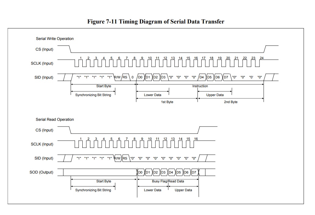
lcdspi.jpg
 
Last edited:
I put a connector on the board so that I can use the logic analyzer as an SPI monitor. From that, I can see that I have something
wrong with the polarity and phase of the SPI clock.

The other thing is the data transfer. I'm sending high nybble first, then low nybble.

I'm going to do some tests this morning (Morning here...coffee time. :) )

Will let everybody know. :)
 
I can't swear to it, but I have a feeling that you must actively use the /CS input to start and end each bus transaction...
 
Here's my transmitter code.

Code:
            .equ    SPICommand,        #0xf8
            .equ    SPIData,        #0xfa
            .equ    SPIRcvData,        #0xfc
;
; SPI2Send:
;           W0: Data byte to send
;           W1: Command or Data
;
_SPI2Send:
                            mov.w    W1,W2
                            swap    W0                ;
                            clr.b    W0                ; Clear the upper byte of the command word
                            swap    W0                ;
                            mov.w    W0,W1            ; Save a copy

                            mov        W2,SPI2BUF        ; Write the command preamble to SPI2
_SPI2Send1:
                            mov        SPI2STAT,W0        ; Wait for transmit done
                            btst.z    W0,#1
                            bra        nz,_SPI2Send1

                            mov        W1,W0
                            and.b    W0,#0x0f,W0
                            swap.b    W0
                            mov        W0,SPI2BUF
_SPI2Send2:
                            mov        SPI2STAT,W0
                            btst.z    W0,#1
                            bra        nz,_SPI2Send2

                            mov        W1,W0
                            swap.b    W0
                            and.b    W0,#0x0f,W0
                            swap.b    W0

                            mov        W0,SPI2BUF
_SPI2Send3:
                            mov        SPI2STAT,W0
                            btst.z    W0,#1
                            bra        nz,_SPI2Send3

                            repeat    #32
                            nop
                            return

Usage:
Code:
            mov.w    #0x0034,W0
            mov        #SPICommand,W1
            call    _SPI2Send

rjenkinsgb: You may be correct. It doesn't seem to make any difference though.
 
MJ .. Display solved ? From the chart above , the SPI interface would appear to be taking 3 bytes then 'addressing ' the LCD driver as a 4 bit device, I presume that is how your sending controls and data ..?

mov.w #0x0034,W0

Would suggest an 8 bit data entry ?

My raw LCD init stream starts with h'33 ( 8 bit mode ) h'28 (4 bit mood :) {0x33,0x32,0x28,0x08,0x0C,0x06,0x01};
control.jpg
 
Last edited:
granddad: It's worse than that. I did some snooping yesterday.

Their example is -very- wierd. It looks like they're doing a software SPI implementation. (???)

But it tells me a lot about the display unit, and what's needed to get it working.

Take a look at this code.

Code:
//-----------------------------------------------------------------------------------------
// Portkonstanten

#define DMRESPORT    PORTA
#define DMRES        0
#define DMCSPORT    PORTA
#define DMCS        1
#define DMCLKPORT    PORTA
#define DMCLK        2
#define DMSIDPORT    PORTA
#define DMSID        3
#define DMSODPIN    PINA
#define DMSOD        4


//-----------------------------------------------------------------------------------------
// Funktions Makros

#define SetBit(adr, bnr)    (  (adr) |=  (1 << (bnr))      )
#define ClrBit(adr, bnr)    (  (adr) &= ~(1 << (bnr))      )
#define EorBit(adr, bnr)    (  (adr) ^=  (1 << (bnr))      )
#define TstBit(adr, bnr)    ( ((adr) &   (1 << (bnr))) > 0 )


//-----------------------------------------------------------------------------------------

void SPIout(char out)
{
  char i = 8;
  
  while(i-- > 0)
   { ClrBit(DMCLKPORT, DMCLK);
     if(out & 1)
        SetBit(DMSIDPORT, DMSID);
     else
        ClrBit(DMSIDPORT, DMSID);
     out >>= 1;
     _NOP();
     _NOP();
     SetBit(DMCLKPORT, DMCLK);
   }
}

char SPIin(void)
{
char i = 8, in = 0;
  
while(i-- > 0)
{
    ClrBit(DMCLKPORT, DMCLK);
     _NOP();
     _NOP();
     _NOP();
     _NOP();
     _NOP();
     SetBit(DMCLKPORT, DMCLK);
     in >>= 1;
     if(TstBit(DMSODPIN, DMSOD))
        in |= 0x80;
   }

  return in;
}

//-----------------------------------------------------------------------------------------

void lcdbefout(char out)
{
  ClrBit(DMCSPORT, DMCS);
  SPIout(0x1F);
  SPIout(out & 0x0F);
  SPIout(out >> 4);
  SetBit(DMCSPORT, DMCS);

  if(out > 0  &&  out < 4)
     waitms(3);
  else
     waitus(50);
}

void lcddatout(char out)
{
  ClrBit(DMCSPORT, DMCS);
  SPIout(0x5F);
  SPIout(out & 0x0F);
  SPIout(out >> 4);
  SetBit(DMCSPORT, DMCS);

  waitus(50);
}

//-----------------------------------------------------------------------------------------

GLOBAL void LcdClr(void)
{
  lcdbefout(0x01);        // Display l”schen
}

GLOBAL void LcdInit(void)
{
  ClrBit(DMRESPORT, DMRES);
  waitms(2);
  SetBit(DMRESPORT, DMRES);
  waitms(50);

  lcdbefout(0x34);        // Function Set: 8-Bit, Bit RE=1
  lcdbefout(0x09);        // ext. Function Set: 4 Zeilen Modus
  lcdbefout(0x30);        // Function Set: 8-Bit, Bit RE=0
  lcdbefout(0x0C);        // Display On/Off: Display ein, Cursor aus
  lcdbefout(0x06);        // Entry Mode Set: Cursor Auto-Increment

  LcdClr();
}

I had to redo the display connector to add provisions for a reset line. I should have that finished today.

Please correct me if I'm wrong. With a crystal of 32 Mhz, Fcy should be 16 Mhz. That means that each nop should be about 62.5 ns.

That means 16 nops should give me a delay of 1 us.

If I'm right, that's how I'll build my delay routines. :)
 
Please correct me if I'm wrong. With a crystal of 32 Mhz, Fcy should be 16 Mhz. That means that each nop should be about 62.5 ns. That means 16 nops should give me a delay of 1 us.

Looks good . pic24s have 2 clocks per cycle. the code init for 8 bit LCD data length ? but the chart suggest 4 bit . you can read busy ready if delays get too Yuck ... some commands need loads of time ( h'01 clear LCD )
 
Last edited:
TBH I'm not sure at this point. There's another question that gets raised;

To read status, you'd send five '1's, followed by the R/W bit and the RS bit. You would think that the proper byte to write
would be #0xf8 for status.

They're writing it in reverse-order. (0x3f)

That's something that needs to be looked into. ;)

rjenkinsgb may be right. The CS may be needed to start and stop transactions.

Once I nail all of this stuff down, I'm going to create a post with all of the pertinent info.

Then, everybody will be able to benefit from the research. :)
 
I'm so frustrated with this display. No matter what I try, nothing seems to work.
At this point, I'm not sure if the display is blown up.

I sent an email off to the company with details of what I'm doing.
Hopefully, they'll spot something and let me know.
 
I think I might have made some headway. This subroutine seems to get data from the display.

Code:
_SPI2GetStatus:
                            mov        #0x8000,W0
                            mov        W0,SPI2STAT
                            mov        #0x003f,W0        ; This is the command word.
                            mov        W0,SPI2BUF
_SPI2GetStatus1:
                            mov        SPI2STAT,W0
                            btst.z    W0,#1
                            bra        nz,_SPI2GetStatus1

                            clr.w    W0
                            mov        W0,SPI2BUF
_SPI2GetStatus2:
                            mov        SPI2STAT,W0
                            btst.z    W0,#1
                            bra        nz,_SPI2GetStatus2
_SPI2GetStatus3:
                            mov        SPI2STAT,W0
                            btst.z    W0,#0
                            bra        z,_SPI2GetStatus3
                            mov        SPI2BUF,W0
                            return

In my reset code, I set the OE to low and left it there. So it only needs to be low to address the display unit.

There are a few things that need to be pointed out:

1 ) The command word is a mirror image of what is implied in the data sheet. That may be due to how SPI works.
I really don't know that much about it. Looking at the timing on the logic analyzer is confusing because it does not match the
documentation. But it appears to work (?)

2 ) After sending the command word, you -need- to send a zero. Then and only then will the display send the status.

3 ) The return value is also reversed. That means bit #0 is the actual status bit.

This is what I've found so far. Next, I'll attempt to apply what I've learned to the command transmitter routine.

More to follow...
 
SPI can be sent either MSB or LSB first. So it looks like you have two devices that don't use the same bitness(??). I know pics default to MSB first - does that help with the timing diagram?

Mike.
 
MJ , Guess those LCD wont be flying off the shelf :(. There seems little advantage using the SPI ? There are some character LCD designs just using an 8 bit shift register . I have used an I2C port expander MCP23008 / 17 ( MC do an SPI port expander ) and tried a pack pack module , but found making my own back pack much better .
 
SPI can be sent either MSB or LSB first. So it looks like you have two devices that don't use the same bitness(??). I know pics default to MSB first - does that help with the timing diagram?

Mike.

Pommie: That explains why the command byte needs to be backwards.

Yesterday (what seems to be a few hours ago. :eek: ) I sent an email off to Electronic Assemblies.

Their turnaround is lightning fast!

Herr Demmel suggested that my SPI baud rate may be too fast. I'm going to look into that today.

(After my first cup of coffee. :D )

MJ , Guess those LCD wont be flying off the shelf :(. There seems little advantage using the SPI ? There are some character LCD designs just using an 8 bit shift register . I have used an I2C port expander MCP23008 / 17 ( MC do an SPI port expander ) and tried a pack pack module , but found making my own back pack much better .

They look like really nice display units. If I can't get this working, it would be a shame. :(
 
So I built a "bit-banger" serial interface.

Here's the source code, in case anyone wants to take a look

Code:
                    .equ __24F32KA304,1
                    .include "p24F32KA304.inc"

                    .text

                    .global _SPIInitialize
                    .global _SPISendCmd
                    .global _SPISendData
                    .global _SPIGetStatus
                    .global _Delay_US

                    .equ    OELine,#9
                    .equ    SDILine,#3
                    .equ    SDOLine,#4
                    .equ    SCKLine,#5

                    .equ    SCLKDelay1,#64    ; 32 = 23.15uS
                    .equ    SCLKDelay2,(SCLKDelay1 + #13)

_Delay_US:
                    repeat    #14
                    nop
                    dec        w0,w0
                    cp        w0,#0
                    bra        gt,_Delay_US
                    return

_SPIInitialize:
                    mov.w    #0x1800,w0
                    mov.w    w0,SPI1CON1
                    nop

                    clr.w    w0
                    mov.w    w0,SPI1CON2
                    nop

                    mov        #0x8000,W3
                    mov        W3,SPI1STAT

                    mov.w    #0x1800,w0
                    mov.w    W0,SPI2CON1
                    nop

                    clr.w    W0
                    mov.w    W0,SPI2CON2
                    nop

                    mov        #0x8000,W3
                    mov        W3,SPI2STAT

                    bset    LATA,#11    ; Set Reset high...
                    call    _SPI2Reset
                    return

_SPI2Reset:
                    bset    LATA,#OELine        ; Set OE high...
                    bclr    LATC,#SDOLine        ; Set SOUT low...
                    bset    LATC,#SCKLine        ; Set SCLK high...
                    return

_SPISend:
                    clr.w        w2                ; Reset the loop counter...
                    mov            PORTC,W8        ; Grab a copy of PORT C
_SPISend1:
                    ior            #32,W8            ;
                    xor            #32,W8            ; SCK = 0
                    btst.z        W0,#0
                    bra            nz,_SPISend2
                    ior            #16,W8            ;
                    xor            #16,W8            ; Clear SOUT
                    goto        _SPISend3
_SPISend2:
                    ior            #16,W8            ; Set SOUT
_SPISend3:
                    mov            W8,LATC
                    repeat        #SCLKDelay2
                    nop
                    xor            #32,W8            ; Toggle SCK...
                    mov            W8,LATC
                    repeat        #SCLKDelay1
                    nop
                    rrnc        w0,w0
                    inc            w2,w2
                    cp            w2,#8
                    bra            lt,_SPISend1
                    bclr        LATC,#SDOLine
                    bset        LATC,#SCKLine
                    return

_SPIRcv:
                    clr.w        w0                ; Clear result...
                    clr.w        w2                ; Reset the loop counter...
                    mov            PORTC,W8        ; Grab a copy of PORT C
_SPIRcv1:
                    ior            #32,W8            ;
                    xor            #32,W8            ; SCK = 0
                    btst.z        W0,#0
                    bra            nz,_SPIRcv2
                    ior            #16,W8            ;
                    xor            #16,W8            ; Clear SOUT
                    goto        _SPIRcv3
_SPIRcv2:
                    ior            #16,W8            ; Set SOUT
_SPIRcv3:
                    mov            W8,LATC
                    repeat        #SCLKDelay2
                    nop
                    xor            #32,W8            ; Toggle SCK...
                    mov            W8,LATC
                    repeat        #SCLKDelay1
                    nop
                    rrnc        W0,W0
                    btst.z        W8,#SDILine
                    bra            z,_SPIRcv4
                    ior            #128,W0
_SPIRcv4:
                    inc            w2,w2
                    cp            w2,#8
                    bra            lt,_SPIRcv1
                    bclr        LATC,#SDOLine
                    bset        LATC,#SCKLine
                    return

_SPISendCmd:
                    bclr        LATA,#OELine
                    nop
                    nop
                    nop
                    nop
                    swap        W0
                    clr.b        W0
                    swap        W0
                    mov.w        W0,W1
                    mov            #0x001f,W0
                    call        _SPISend
                    mov            W1,W0
                    and.b        W0,#0x0f,W0
                    call        _SPISend
                    mov            W1,W0
                    swap.b        W0
                    and.b        W0,#0x0f,W0
                    call        _SPISend
                    bset        LATA,#OELine
                    return


_SPISendData:
                    bclr        LATA,#OELine
                    nop
                    nop
                    nop
                    nop
                    swap        W0
                    clr.b        W0
                    swap        W0
                    mov.w        W0,W1
                    mov            #0x005f,W0
                    call        _SPISend
                    mov            W1,W0
                    and.b        W0,#0x0f,W0
                    call        _SPISend
                    mov            W1,W0
                    swap.b        W0
                    and.b        W0,#0x0f,W0
                    call        _SPISend
                    bset        LATA,#OELine
                    return

_SPIGetStatus:
                    bclr        LATA,#OELine
                    nop
                    nop
                    nop
                    nop
                    mov            #0x003f,W0
                    call        _SPISend
                    call        _SPIRcv
                    bset        LATA,#OELine
                    return
.end

Please let me know if you spot anything silly. :)

I'll be testing this over the next few days...
 
granddad: Thanks. TBH, this is my first PIC project. I have worked on other processors before, (8085, 80186EB)
but never the PIC. And I think I chose one of the more difficult ones; one that was the least used.

There are so few code examples out there.

BTW: heartfelt thanks to all who have been involved in helping me to struggle through this.

I'm grateful. :)

Well...back to the keybed scan code. With a working display, I can see what the data looks like.
This will also be invaluable for testing the A/D converters.

The saga continues...
 
I have updated the schematic and the firmware.

Post #143 has the updated schematic and Post #154 has the latest firmware.
 
You have 4 unused logic gates of the 74HC14.
You can use it to implement a MiDi thru, when You need one for Your Keytar.
 
Status
Not open for further replies.

Latest threads

New Articles From Microcontroller Tips

Back
Top