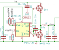
Part is NCP81151. The boostrap is fed internally by diode to VCC, which is VBUS. Input is 0-40V.
Consider the system has been in sleep and turns on. The output is already near VBUS. An input voltage presents itself and the MCU sends a PWM to the input. The 81151 is in auto diode emulation mode. The bootstrap doesn't charge through either the lower FET or the output (which is too close to VCC) and subsequently the converter fails to start switching.
I've been going around in circles with this one.
1. ditch it and go PMOS on highside, which is more challenging to drive when factoring in gate protection.
2. create a voltage doubler and feed to the NCP81161 which iirc is rated about 17v (though current consumption is double), so Vgs will always be v=BST-load.
3. try to do the same using a buck all-in-one, though I'm curious how they resolve it or if it's a systemic issue with the NMOS highside design.
4. blip the lowside NMOS off briefly at the start of operation to allow BST to charge, and do it quickly to ensure reverse flow doesn't fry the FET. This won't help if the NCP81151 switches low side to diode emulation later on (wouldn't know).
5. Stick a detect on the lowerside FET, if the output voltage is close to VCC (MCU measures it) and this FET hasn't been turned on in a while then do the blip of (4).
6. Something else?..

