Continue to Site

Welcome to our site!

Electro Tech is an online community (with over 170,000 members) who enjoy talking about and building electronic circuits, projects and gadgets. To participate you need to register. Registration is free. Click here to register now.

  • Welcome to our site! Electro Tech is an online community (with over 170,000 members) who enjoy talking about and building electronic circuits, projects and gadgets. To participate you need to register. Registration is free. Click here to register now.

Buck Boost with 555

Status
Not open for further replies.

polashd

Member
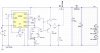
I'm designing a buck-boost converter using 555 ic (see attached pic).
While simulating in Ltspice it shows that the Mosfet (N-channel) is always conducting (simulation pic attached), as a result the current is not going to the Load. It doesn't happen if P-channel mosfet is used. I can't understand why it's behaving like this. When the gate is discharged /ground the N-mosfet is supposed to turned off.

I get this only with buck-boost design. For boost converter design the mosfet behaves normal. Is it a problem of my design or it's because of Ltspice?

*One more help I need is - I want to use it as regulated current source. In a non-inverting output it can be done easily by adding a series resistor before ground, the dropped voltage will bias an npn which pulls down the CV pin of 555 and turn off the IC.
How can I do this in a inverting buck-boost design.
 

Attachments

  • Buck-Boost with 555 a.JPG
    Buck-Boost with 555 a.JPG
    87 KB · Views: 840
  • Buck-Boost with 555 b.JPG
    Buck-Boost with 555 b.JPG
    81.8 KB · Views: 406
Read this

The leds on the output need to have current limiting.
 
When the gate is discharged /ground the N-mosfet is supposed to turned off.
Not quite. You also have to consider the source voltage. For the FET to turn off, Vgs should be less than the Vgs(thr) threshold value. In your circuit, the source is being driven negative, so Vgs is remaining above Vgs(thr) even when the gate is at 0V.
 
Last edited:
POST Issue2 of 2016_11_30

Hi polashd,

below is a circuit you may find will do your job.

spec

2016_11_28_Iss3_ETO_LM555_FLYBACK_CONVERTER_VER1.jpg
 
Last edited:
below is a circuit you may find will do your job.

I've never thought of using a 555 that way. That's rather clever. :cool:
 
Not quite. You also have to consider the source voltage. For the FET to turn off, Vgs should be less than the Vgs(thr) threshold value. In your circuit, the source is being driven negative, so Vgs is remaining above Vgs(thr) even when the gate is at 0V.
thanks. That solves what was a mystery to me.
But this should be common in this type of circuit. How it's handled in buck-boost topology (where mosfet is N-channel)
 
How it's handled in buck-boost topology (where mosfet is N-channel)
The TI pdf I linked you to shows how. The IC they use has a "charge-pump"capability that stores the voltage (greater than the input voltage, 10V in your circuit) and boosts the gate drive for the NFet to almost twice the input voltage. i.e., the gate drive for the NFet goes to almost 20V when your 555 is constrained to less than 10V!
 
The TI pdf I linked you to shows how. The IC they use has a "charge-pump"capability that stores the voltage (greater than the input voltage, 10V in your circuit) and boosts the gate drive for the NFet to almost twice the input voltage. i.e., the gate drive for the NFet goes to almost 20V when your 555 is constrained to less than 10V!

That will give the N-channel mosfet a better turn on, but doesn't solve the problem of turning the mosfet off.

When the output of the 555 turns off and the gate voltage goes to ground, the inductor voltage reverses. This takes the source pin of the mosfet negative, so the mosfet turns on again. This effectively camps the source at the Vgs level below ground until the mosfet turns on again.

The easiest way to do this type of converter is with a p-mos device. To use a n-mos device, you need to either use an isolated gate driver, or connect the 555 so that it's ground is common to the n-mos source, but not common to the input ground.

polashd, what is your reason for wanting to use an n-mos instead of a p-mos device?


My apology to MikeMl. The link you provided does address the points I made.
 
I've never thought of using a 555 that way. That's rather clever. :cool:
Very clever indeed!

Yet ANOTHER useful 555 circuit. Probably the most versatile linear IC ever made.
Thanks TCM and ST, but it is a pretty standard flyback converter.

The configuration shown, is a bang, bang converter: the converter goes flat out for a few cycles and then stops when the transistor turns on. The converter then starts up again when the transistor turns off. It is only a skeleton circuit and has not been optimized.

A pulse width modulated version is a bit more complicated, but not much.

Yes, the 555 is a very popular chip, as you say ST: a billion 555s are made every year.:cool:

spec
 
It seems to be a boost converter. I need buck-boost (with current limiting in a similar way).
No, the circuit of post #4 is a buck, boost converter: the output voltage (or current) can go from roughly 0V to infinity volts (in theory of course).:)

The current through the LED string (Iled) is defined by 0.6V/Ri or, rearranging, Ri = 0.6V/Iled

If you are interested in using this approach, you should be aware that the sketch shown in post #4 is just a skeleton circuit for you to develop. Although the circuit as it stands will work, a bit of hysteresis in the current detector (transistor) would be wise.

Also, the NMOSFET gate drive resistor, while probably fine, should really be optimized for the actual NMOSFET you use. You can also use an NBJT in place of the NMOSFET, for low power conversion.

You will also need to do the inductor calculations to suit your requirement.

spec
 
polashd, what is your reason for wanting to use an n-mos instead of a p-mos device?
As I know N-mos are easier to work with(and easy to find in my local stores) and has lower Rds(on). Also I have some in my stock.

- I still need help for current limiting method for buck-boost.
can you suggest .
 
As I know N-mos are easier to work ...

NMOSFETs and PMOSMETs are equally easy to use and, these days, PMOSFETs approach the performance of NMOSFETS.:)

With an NMOSFET you just make the gate more positive than the drain and the NMOSFET will conduct current (in both directions) between its drain and source.

With a PMOSFET you just make the gate more negative than the drain and the PMOSFET will conduct current (in both directions) between its drain and source.

And that is all there is to it.:cool:

spec
 
As spec said, driving the two are about the same. The difference is how they are being used. In your application, a p-mos device will be easier to use. I do understand your issue with part availability. An n-mos can be used, but will require extra components, so there is a trade-off of which is really easier in the end.

As for working up a design for you, we need more information.
What is the input voltage range?
What output current do you need, across what output voltage range?
 
It seems to be a boost converter. I need buck-boost (with current limiting in a similar way).
Why do you need buck-boost?
What is the input voltage range?
 
No, the circuit of post #4 is a buck, boost converter: the output voltage (or current) can go from roughly 0V to infinity volts (in theory of course)
I don't see how. :confused:
If the MOSFET turns off for any length of time, then the output will charge to the supply voltage minus the diode drop.
How can the output go below the supply voltage?
 
I don't see how. :confused:
If the MOSFET turns off for any length of time, then the output will charge to the supply voltage minus the diode drop.
How can the output go below the supply voltage?
That's what I was trying to say in my post (#8)
Can anyone pls explain how the circuit in post#4 will behave as a buck-boost.
 
Status
Not open for further replies.

Latest threads

New Articles From Microcontroller Tips

Back
Top