Continue to Site

Welcome to our site!

Electro Tech is an online community (with over 170,000 members) who enjoy talking about and building electronic circuits, projects and gadgets. To participate you need to register. Registration is free. Click here to register now.

  • Welcome to our site! Electro Tech is an online community (with over 170,000 members) who enjoy talking about and building electronic circuits, projects and gadgets. To participate you need to register. Registration is free. Click here to register now.

Buck Boost with 555

Status
Not open for further replies.
I don't see how. :confused:
If the MOSFET turns off for any length of time, then the output will charge to the supply voltage minus the diode drop.
How can the output go below the supply voltage?
That's what I was trying to say in my post (#8)
Can anyone pls explain how the circuit in post#4 will behave as a buck-boost.

Yes, my error. The inductor needs to have a secondary winding. I had transposed from an inverting buck/boost inverter, using a PMOSFET, without realizing the consequences.

As it stands, the circuit of post #4 is a boost controller only.

spec
 
Last edited:
Modifying Mr. Spec's drawing:
If you want the output voltage to be more/equal/less than the input voltage then:
L1 kicks up through D1 to produce a voltage on the LEDs. (note the LEDs are not on ground but the supply)
When the LED current reaches a point it will turn on Q-PNP. (Base is on supply. When the Emitter is above supply by 0.65V the transistor will turn on.)
When Q-PNP is on it will turn on Q1 and turn 555 off.
---edited---
Probably should make R4 (bottom right) a 10k resistor. OR Make R4 (top right) a 100 ohm resistor.
upload_2016-11-29_22-48-49.png
 
Pretty neat Ron:cool:

That approach would have been so useful for previous designs I have messed with.:)

I also updated the circuit of post #4 to make the converter buck/boost (I hope).

spec
 
Last edited:
You could configure the 555 as a monostable, and use the reset i/p to form an astable oscillator based on current sensed on the o/p, similar to a current mode switching controller.
 
You could configure the 555 as a monostable, and use the reset i/p to form an astable oscillator based on current sensed on the o/p, similar to a current mode switching controller.
Yes DP, you mean do a proper job- but I am too lazy for that.:)

spec
 
Last edited:
Below is the outline circuit I started with (timing components and decoupling capacitors not shown), but then got a bit careless transposing from a PMOSFET to an NMOSFET.:banghead:

spec

2016_11_30_Iss1_ETO_555_INVERTING_BUCK_BOOST_CONVERTER.jpg
 
Last edited:
Hi all,

I think the circuit below may do the job (buck/boost with NMOSFET)

spec

2016_12_01_Iss1_ETO_555_BUCK_BOOST_INVERTER_CONSTANT_I_VER4.png
.​


I'm designing a buck-boost converter using 555 ic
So this project is to make a 555 do a job it was never intended to do. Thanks to Mr. Spec's cleverness it works.
A buck/boost is hard. The idea of any input voltage and any output voltage is what makes it hard(er).

Here is a boost I have used in several projects. I used it as a back light driver in several pieces of test equipment. Vin must be smaller than Vout.
Vin 2.7 to 16V, Vout <30V. Small SOT23 6-pin IC. Notice the low part count when you use a IC built to do the job.
upload_2016-12-1_17-53-29.png

Here is a buck. Again all in a SOT23 5-pin IC.
Vin<Vout
Vin 4.5 to 40V 1.0 and 1.5A versions.
I have not used this AL8860 but we are shipping millions a year of its older brother. The entire circuit is small so it fits inside a flash light bulb.
upload_2016-12-1_18-0-49.png

Here is a picture of a flashlight bulb. You can see the SOT23 IC + external transistor + diode + cap. The other side the board has a coil + cap. This is a "boost/buck" in that the input and output voltages do not have restrictions. The transistor and diode could have been saved if this was boost or buck only.

upload_2016-12-1_18-20-56.png
 
Hi all,

I think the circuit below may do the job (buck/boost with NMOSFET)

spec


Great circuit, using a well known 555 timer chip. Can you give some instructions (calculation formula) how to calculate the inductor value? I'd like to drive 4 CREE XML T6 (~12V output) with 210-300 mA. The input voltage varies between 6-12 Volts. Thanks.
 
Ron Dekkers site shows you how to design a very similar circuit, only he uses the control input instead of the reset, the circuit doesnt have the constant current driver as its a high voltage supply, but it can easily be adjusted for lower voltages.
https://www.dos4ever.com/flyback/flyback.html
Note Ron' s circuit is a boost, I've used this circuit for either buck or boost.
 
I just registered to say thank you for that very useful write up!

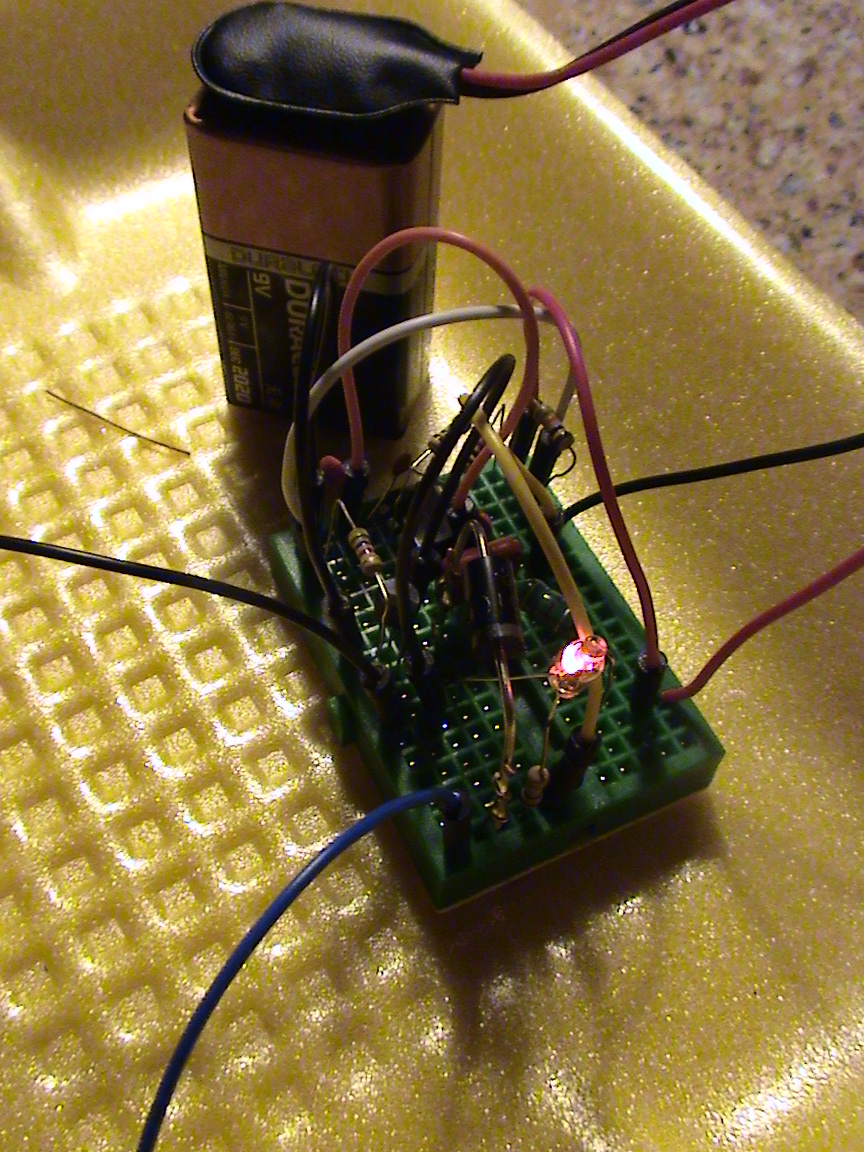
I had a breadboard with a half finished boost converter to power an NE-2 clone neon glow lamp from a 9 V battery when I found that web page via this forum. If I have questions, do you have a preferred thread to ask them in?

Ron Dekkers site shows you how to design a very similar circuit, only he uses the control input instead of the reset, the circuit doesnt have the constant current driver as its a high voltage supply, but it can easily be adjusted for lower voltages.
https://www.dos4ever.com/flyback/flyback.html
Note Ron' s circuit is a boost, I've used this circuit for either buck or boost.
 
Pleased to help.
I've forwarded loads to rons page, I should contact him.
I built one of his inductor test jigs years back, I modded it to work better on an old 'scope, and I use it a lot.
 
The boost converter I'm building is similar to the one in Fig. 3 on the web page you linked to ("Simple 12-180V boost converter using the 555 as controller"). However, since my input voltage is provided by a 9V battery, there is no voltage ripple and I assume the C1 and C2 caps would serve no purpose?

Also, I will only need about 100V output voltage and very low current (about 0.1mA). Do I really need a power transistor, or could I get away with using a regular high-voltage NPN transistor, such as A42 (rated for 300V) or even 2N5551 (160V)? I have both the latter available.

Pleased to help.
I've forwarded loads to rons page, I should contact him.
I built one of his inductor test jigs years back, I modded it to work better on an old 'scope, and I use it a lot.
 
100v at 0.1ma is about 10ma plus inefficiencies at 12v, so an mpsa42 might do the trick, the thing to take note of is the output cap, if its only small then the mpsa42 ought to cope.
There will be some heating of the device due to base current and base emitter capacitance, also take care of the switch off ringing this can destroy the switching device by over volting, a vdr helps here maybe a little lower voltage rating than the vce max of the transistor, lash it up & try it.
 
Excellent.
Seeing as your using a single inductor you probably dont need a snubber or vdr on the transistor, so long as you used an ultra fast diode.
I dont see an output capacitor on that circuit, I'm surprised that works without it, a 100n high voltagecap across the neon woudl make the circuit more efficient and brighten up the neon.
 
There is an output cap. It's the brown component (salvaged from a broken CFL) behind the diode. The yellow wire puts it across the load. I actually think I used the 100 nF you suggest, but I'll check.

Can you elaborate on your "snubber or vdr on the transistor" comment? I do use a Schottky diode (SB5100), but I'm very interested to understand potential issues when not using a single inductor. I might want to try a flyback transformer in a future iteration. Would that warrant using a snubber or vdr? I don't know what either of those are!
 
Ok.
There are some parasitics involved in the switch section, the parasitic capacitance of the transistor rings with the leakage inductance of the inductor when the transistor switches off, this is usually worse with a 'transformer' or coupled inductor as it should be called.
This ringing can exceed the power supply rail or more, on some topologies the switch already 'sees' twice the supply rail so ringing can easily take the tranny above its voltage rating and blow it.
An Rc snubber is just a series rc across the transistor or across the inductor, the r is chosen so that the voltage across the inductor at switch off pushes the same current through the resistor as that through the switching tranny at full load, then initially the cap is chosen to soak up the energy stored by the parasitic capacitance, a common way of doing this is chucking caps across the tranny till the ringing frequency halves, then I think you quadruple that capacitance and that becomes the c part of the rc.
I tend to calc the r and bung various caps on and scope the result, a few goes and its sorted.
You can put a diode inline with the rc so it becomes a drc, and put a high value r across the c to discharge it when the diode isnt conducting, this then only burns power at switch off making it more efficient, there are more elaborate and low loss ideas too.
A Vdr stands for voltage dependant resistor, this is a resistor that suddenly lowers its resistance at its marked voltage, then when wired in a circuit if the voltage tries to spike to a higher voltage than that marked on the vdr it tries to short the spike by lowering its resistance and clamping the voltage from rising too high, either the vdr damps the spike, or it blows up.
You can also use a zener diode in series with a diode, or a transorb, all similar ideas.
That was just a ballpark description aimed to be understandable, other ideas may well follow.
 
I really appreciate all the sage advice! I'm planning to do some ngspice simulations while I wait for the boat from Shenzhen to arrive with better inductors.
 
Status
Not open for further replies.

Latest threads

New Articles From Microcontroller Tips

Back
Top