StopGo
New Member
I decided to give it a go again, using the laser toner transfer method.
First a quick trip into town to buy some materials..
- single sided copper clad PCB
- a big blue tray
- a bottle of FerricChloride
- an etch resistant pen (a bog standard stadler permanent marker)
- a polishing block for the copper
- 0.8mm drill for my dremmel
- nail polish remover (acetone)
I need a new NiCd charger, and it seemed an ideal thing for this test.
**broken link removed**
I quickly sketched out my circuit schematic in Multisim9. The general plan.. a 230v to 12v AC transformer, full bridge rectifier, a big cap, and then a Power transistor current source with integral LED charge indicator. (The transformer is not PCB mounted) Once happy with it, I tried exporting the schematic into ExpressPCB, but it didn't seem to cope with any of the obvious export formats. Perhaps if I had kept at it I would of found one. I gave up in the end.
So I started from scratch with a blank PCB in ExpressPCB. First I resized the workspace to match my PCB. In the excitement I had rushed ahead and chopped off a small 2" by 1.25" piece of board thinking I have seen so many charger circuits before, that I knew how big it should be. The polishing block, looks like a grit filled eraser. seemed to do a good job of making the copper look clean, so I just brushed the dust and grit away with a clean paint brush once I was done.
I added my various components and pads onto the PCB, then joined the dots, and added a little text too, it all seemed to fit I printed out a test on plain paper. Perfect match for size, and everything looked well within the capabilities of my little laser printer.. but then frustration sets it.
ExpressPCB won't let me print a mirror image of my circuit!!
Some head scratching, then an idea.. 5 minute google... I find some software called "Zan Image Printer". This little gem is a virtual printer driver that captures what you print as image files. I print my circuit to the "Zan Image Printer", but it comes out blocky and pixilated due to being captured actual size with only 300dpi res. More head scratching.. ExpressPCB has an option to "resize to fit page" checkbox, course this makes the PCB way too big, but photo shop soon reduces things back to wanted size, and with no loss of detail. ExpressPCB prints a thin box where the edges of the PCB are, this is an ideal guide for cropping the enlarged image before reducing it to whatever size your PCB is.
I printed the PCB design on Photo quality glossy inkjet paper, fed manually into my laser printer. Glossy paper has no fibres like normal paper, the toner seems to sit on top and even has a visible profile when viewed side on.
I put some newspaper down on the kitchen workbench, put the copper board on it, cut the print to size and laid it on the copper board, finally a single sheet of A4 over the top. Then used my clothes iron on full power for about 3-4 minutes just pressed down flat on the whole lot. It did get hot enough for the paper to brown a little. I went round the edges with the tip of the iron for good measure. The heat had made the glossy paper back stick to the single sheet of A4, it wasn't coming off.
After the ironing, I plunged the PCB into water and left it for 10 minutes. I was expecting the paper to become soft but the photo paper had a plastic backing layer and was very resistant to the water, in the end I had to just peel it off. (Epson premium glossy)
This seemed to work mostly, but some of the fine text at the side failed to stick to the copper, and one track in the middle needed touching with the pen. Without further pause, I poured the etching solution into the tray, then in went the PCB. It took 5 minutes of poking it with a kebab stick before the copper finally vanished leaving just the tracks. The etch pen had worked just as well as the laser toner.
The toner was difficult to remove, even with "scotch brite" scour pads and the acetone, but it did eventually clean up.
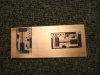
So here it is.. the finished artifact..
**broken link removed**
**broken link removed**
First a quick trip into town to buy some materials..
- single sided copper clad PCB
- a big blue tray
- a bottle of FerricChloride
- an etch resistant pen (a bog standard stadler permanent marker)
- a polishing block for the copper
- 0.8mm drill for my dremmel
- nail polish remover (acetone)
I need a new NiCd charger, and it seemed an ideal thing for this test.
**broken link removed**
I quickly sketched out my circuit schematic in Multisim9. The general plan.. a 230v to 12v AC transformer, full bridge rectifier, a big cap, and then a Power transistor current source with integral LED charge indicator. (The transformer is not PCB mounted) Once happy with it, I tried exporting the schematic into ExpressPCB, but it didn't seem to cope with any of the obvious export formats. Perhaps if I had kept at it I would of found one. I gave up in the end.
So I started from scratch with a blank PCB in ExpressPCB. First I resized the workspace to match my PCB. In the excitement I had rushed ahead and chopped off a small 2" by 1.25" piece of board thinking I have seen so many charger circuits before, that I knew how big it should be. The polishing block, looks like a grit filled eraser. seemed to do a good job of making the copper look clean, so I just brushed the dust and grit away with a clean paint brush once I was done.
I added my various components and pads onto the PCB, then joined the dots, and added a little text too, it all seemed to fit I printed out a test on plain paper. Perfect match for size, and everything looked well within the capabilities of my little laser printer.. but then frustration sets it.
ExpressPCB won't let me print a mirror image of my circuit!!
Some head scratching, then an idea.. 5 minute google... I find some software called "Zan Image Printer". This little gem is a virtual printer driver that captures what you print as image files. I print my circuit to the "Zan Image Printer", but it comes out blocky and pixilated due to being captured actual size with only 300dpi res. More head scratching.. ExpressPCB has an option to "resize to fit page" checkbox, course this makes the PCB way too big, but photo shop soon reduces things back to wanted size, and with no loss of detail. ExpressPCB prints a thin box where the edges of the PCB are, this is an ideal guide for cropping the enlarged image before reducing it to whatever size your PCB is.
I printed the PCB design on Photo quality glossy inkjet paper, fed manually into my laser printer. Glossy paper has no fibres like normal paper, the toner seems to sit on top and even has a visible profile when viewed side on.
I put some newspaper down on the kitchen workbench, put the copper board on it, cut the print to size and laid it on the copper board, finally a single sheet of A4 over the top. Then used my clothes iron on full power for about 3-4 minutes just pressed down flat on the whole lot. It did get hot enough for the paper to brown a little. I went round the edges with the tip of the iron for good measure. The heat had made the glossy paper back stick to the single sheet of A4, it wasn't coming off.
After the ironing, I plunged the PCB into water and left it for 10 minutes. I was expecting the paper to become soft but the photo paper had a plastic backing layer and was very resistant to the water, in the end I had to just peel it off. (Epson premium glossy)
This seemed to work mostly, but some of the fine text at the side failed to stick to the copper, and one track in the middle needed touching with the pen. Without further pause, I poured the etching solution into the tray, then in went the PCB. It took 5 minutes of poking it with a kebab stick before the copper finally vanished leaving just the tracks. The etch pen had worked just as well as the laser toner.
The toner was difficult to remove, even with "scotch brite" scour pads and the acetone, but it did eventually clean up.
So here it is.. the finished artifact..
**broken link removed**
**broken link removed**
 Oops!
Oops!")
 . He said not the glossy paper, the semi-gloss looking stuff I think.