Well, I played with it some more, and this is the best I could get:
**broken link removed**
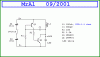
Results as shown (Vo: 10.8V; Io: 49.1mA @ Rl = 220Ω).
Not bad. But I have to say I'm very skeptical of this circuit. Change one component--and not by very much--and it fails to start at all. I actually found best results with a plain Jane 2N2222. If someone can come up with better results I'm prepared to be beaten.
Yes, the absence of a ground may have allowed the circuit to pick up DSCSI, as you described. Funny that LTspice didn't warn me about having no ground as it usually does.
You never answered my question about the oscillator: how exactly does it work?
Do you have LTspice (or another Spice) so you can try my simulation?
Hi Carbon,
I also think you are doing quite well with these circuits BTW.
Earlier when i quoted "100 ohms" i meant the output resistor, not R1, sorry about that.
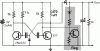
This circuit is quite reliable. There are a few requirements but that goes for any circuit really. For example, the inductor ESR has to be low enough to allow enough current to flow to pull Q2 out of saturation. More about this later.
Try this:
Q2=2N4401
L1=200uH, Resr=0.1 ohms
C2=10uf
RL=33
R1=50
C1=300pf
and note the output current level.
Oh yeah before i forget, if you are generating output voltages that are greater than V1+5 volts (battery voltage plus 5 volts) then you need to add a 1N4148 diode across the base emitter of Q1, so i would suggest adding that for your 9v output.
One of the important things about this circuit is the gain of Q2. If the gain isnt high enough for a particular part number then we wont be able to get enough output current.
To help illustrate this, try connecting another transistor 2N4401 in parallel with Q2, except for the base, which is fed from the collector of Q1 through a second 50 ohm resistor. Change RL to 20 ohms, note the output current level !
This circuit is a little like a multivibrator but it uses not only the capacitor C1 as timing element but also the inductor itself.
When the circuit is first turned on, Q1 turns on via R2 so the collector goes high, turning Q2 on. Q2 turning on pulls the right side of the inductor low and the right side of C1 low. The left side of C1 charges quickly so C1 gets a charge across it with polarity +C- (left side positive right side negative). The inductor has approximately the battery voltage across it, so it begins to conduct current. The current keeps rising and rising, and that means the current through Q2 keeps rising too. Eventually the beta of Q2 and base drive through R1 can no longer keep Q2 in saturation, so the collector voltage starts to rise. As the collector voltage rises, that voltage across the capacitor (which acts like a small battery) adds to the collector voltage so Q1 base voltage rises. Q1 base voltage rises up and cuts off Q1, which means no current to the base of Q2 any longer, which means Q2 shuts off completely. The current through L1 that has built up no longer has any place to go, so the voltage at the right side of L1 shoots up suddenly in an attempt to find a path to discharge through. The voltage goes up high enough to turn diode D1 on which then charges capacitor C2.
As the inductor is dumping its energy through D1, the cap C1 now finds a discharge path through R2. With the right side of C1 quite high now the left side starts to charge toward ground making the charge across C1 now -C+ instead of +C-. Eventually the left side of C1 goes low enough to turn Q1 back on, and the whole process repeats.
Eventually after several of these cycles the charge in C2 builds up to some nominal voltage level so RL gets plenty of current.
The extra diode has to be added for voltages more than 5 volts greater than the battery voltage because as the Q2 collector goes high it pulls the right side of C1 high which pulls the left side even higher, which would reverse bias the Q1 base emitter by more than 5 volts which could destroy it.
One limiting factor is the gain of Q2 and of course the base drive. If Q2 can not stay in saturation long enough the current in L1 can not build up high enough to supply the output with enough energy to drive the load RL. This means lowering R1 increases the output energy and using a high gain Q2 also helps. Using two Q2's in parallel of course increases the output energy two fold.
Since Q2 does have to be pulled out of saturation however because that's part of the way this circuit oscillates, that means that the inductor ESR has to be low enough to allow enough current to build up through the collector. The max current is Vbatt/ESR so the gain has to be low enough to allow that current to pull Q2 out of sat.
Oscillation occurs due to two mechanisms: C1 left side charging low causes turn on, and L1 charging to a high level of current causes turn off. These cycles repeat and that's how it oscillates.
BTW many times you can use a max simulation time of 20ms unless you use a large output cap.
")
")

