Continue to Site

Welcome to our site!

Electro Tech is an online community (with over 170,000 members) who enjoy talking about and building electronic circuits, projects and gadgets. To participate you need to register. Registration is free. Click here to register now.

  • Welcome to our site! Electro Tech is an online community (with over 170,000 members) who enjoy talking about and building electronic circuits, projects and gadgets. To participate you need to register. Registration is free. Click here to register now.

Applying capacitors across AC in various serial/parallel ways using FET's.

Status
Not open for further replies.

ACharnley

Member
Hi,

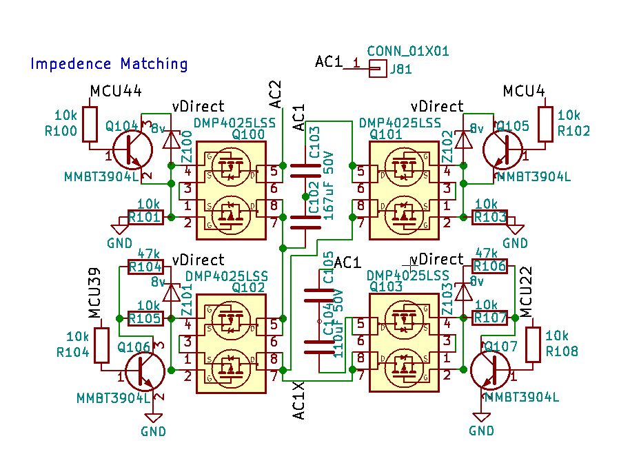
I just want to clarify this circuit looks reasonable without any potential snags.

AC1 and AC2 is 0-40V. AC1X and AC2 go to rectification, so the idea here is to place capacitance in series between AC1 and AC1X and/or in parallel between AC1 and AC2 (and short AC1 and AC1X together). These are;

110uF between AC1 and AC1X
167uF between AC1 and AC2, short AC1 & AC1X
167uF between AC1 and AC1X

FET's don't need to turn on quickly so no drivers required. I have a bit of a fetish for P-channel FET's, but it's because they're high side. The ensure circuit uses 34 P-fets and only 2 N-fets, which makes me wonder if there's anything better.

Vdirect is the rectified voltage. I'm using active rectification so technically the voltage should be nigh on identical to AC1/2, ensuring the FET turns off completely. The zeners prevent under-voltaging the gate. The transistors are because I'm cheap, but also they'll withstand 40V. Q104/5 will thus present a voltage drop but it should be low enough to ensure the FET is off.

Is there an easier way? Triacs would be nice if they didn't have a 0.7V voltage drop. Depleted FET's don't reduce the component count much and usually have reduced performance or higher cost. Any voltage drop is considered make-or-break - a relay is better than a 0.7V drop.

I have no electrical education or background, and I have no idea what I'm talking about. :woot:

Cheers!

Andrew
impedence.png
 
That entire circuit doesn´t make any sense to me. Why are the sources not connected to anything?
Wouldn´t relays be a better and simpler choice?
 
You need a voltage between gate and source to turn a FET on. How will you turn a FET off?
 
kubeek -> forget what they are connected to, just think AC in AC out. vDirect is the rectification of AC out (not shown). Relays are simpler, but are much larger, unreliable long-term and use more power.

alec_t -> they are P-channel so invert your logic. Q102 and Q103 are normally off, Q106 and Q107 drive them to 0V turning on. Q104 and Q105 are the inverse.
 
forget what they are connected to,
No.

Nowhere have you said what the circuit is supposed to *do*. AC what? Electret microphones? Wind farm generators? There are 8 FET sources not connected to anything related to their gates. How do you expect a gates to react when it source is floating? The word vDirect appears 4 times but is not attached to any component or net. What impedance? Matched to what? Why? How do you know when the impedance is unmatched or matched?

I get that you are using back-to-back MOSFETs as bidirectional switches, but only because I have used the technique and recognize your attempt. There is nothing in your posts or in the schematic to indicate that. Also, 40 Vac equals 113 V peak-to-peak. Rethink using 40 V FETs.

A schematic tells the story of a design; there is no award for jamming components into the smallest possible area. I suggest that you redraw the schematic over a larger area and straighten out some of the zig-zaggy lines, so the various circuit elements are arranged to show the signal flow from inputs to outputs, left to right. Show the FETs as individual devices oriented to show how they function in the circuit. Also, label the inputs and outputs. Also, indicate which nets any net names are attached to. There doesn't have to be a tag; having a net name just sit on a net is fine as long as things are spread out enough that it is unambiguous.

ak
 
Last edited:
I think I see what your doing.
The way its connected the gates will more or less act as caps, you'd be charging them when the bjt is on and discharging through the ground resistor when the bjt os off, I'm not sure if that would work though as I dont know if biasing the drain to gate junction would actually switch the fet on.
I think re-arranging the circuit using P and N fets would be more successful, then you can properly drive the gates & have a bipolar signal path, your gate drive circuit would need an extra tranny.
 
Last edited:
I can't post the circuit in it's entirety and voltage levels, impedance, input and output voltages are irrelevant. I should however mention 40V is a mistake, it's clamped lower.

All it is is this:

Two wires carry AC. That's the input.

Two wires carry AC away: That's the output.

Assuming a 100% efficient rectifier across AC gives you vDirect net.

Create a circuit which by way of TTL voltage levels can satisfy the following three conditions;

1. a capacitor can be connected in parallel across the AC.
2. a capacitor can be connected in series with the AC.
3. the same capacitor in (1) can be connected in series with the AC.

The question is, have I succeeded?
 
Last edited:
I have no electrical education or background, and I have no idea what I'm talking about. :woot:
I can't post the circuit in it's entirety and voltage levels, impedance, input and output voltages are irrelevant.
How do you know that those are irrelevant if you say you dont know anything about electronics?
The voltage levels are very relevant, because without them there is no way to properly drive the gate of the fets to turn them on and not destroy them.
 
The fets are driven by the rectified AC, vDirect, which I did mention for this purpose can be considered a 100% efficient conversion.

The transistors will drain the FET's capacitance, it won't be rapid as I'm not using FET drivers, but that's fine here.
 
voltage levels, impedance, input and output voltages are irrelevant.

The question is, have I succeeded?
No. The errors in the post#1 schematic still are there.
Yes, if output voltages are irrelevant.

ak
 
The transistors will drain the FET's capacitance
I don't see how, if the sources are floating. It is Vgs which determines whether a FET is on or off.
 
I don't see how, if the sources are floating. It is Vgs which determines whether a FET is on or off.

The resistors pull them high or low depending on the default. Since vDirect is based on AC the delta is circa 0v. The transistors pull the fet high or low, while the zeners ensure the Vgs doesn't drop more than 8V on vDirect.
 
That actually makes no sense. A mosfet needs voltage between Gate and Source to be about 5-10V for it to turn on. How are you achieving that when voltage at gate pin has no relationship to voltage at source?
 
And ...? P or N channel, still needs gate to be some defined voltage away from souce, be it positive or negative.
 
A P channel turns on fully when the gate is less than source by a determined amount, let's say 5V. For two of the chips the resistors drive the dual FET's gate to ground, turning them on.

For the other two dual FET's, the resistor drives the gate voltage to the same as source (since AC and vDirect are the same voltage). Thus they turn off.

The transistors change the balance depending if high or low side.
 
A P channel turns on fully when the gate is less than source by a determined amount, let's say 5V.
Exactly. And since your sources are not connected to anything directly referenced to the potential at the gates, Vgs is not defined and the circuit will.not.work.

The s in Vgs stands for Source. Vgs is the voltage between the gate and the source, not between the gate and something completely isolated from the source. If the source is floating, it has no electrical relationship with the gate.

Internally, the gate-source structure in an enhancement mode MOSFET is a capacitor. How do you expect to charge up the capacitor when one end is disconnected? In fact, since the capacitor starts out at zero charge, applying 5 V or -5 V or whatever to the gate will just pull the source along with it. The transistor will not conduct because even it the gate voltage changes with respect to ground or some other circuit potential, it is not changing with respect to the source.

ak
 
I'm going to second AnalogKid's request. I'm afraid I can't follow what's going on here - I'm sure you have a valid idea but, like the others, I'm not sure it's quite a working circuit yet.

It would really help if you could re-draw the circuit on a more logical and spacious manner. In particular, it would help if you could show the source and load (no need to specify what they are - just 2 terminal black boxes will do fine) so that we can all see where the current paths are.
If you could also include some sketches of waveforms you think you should see on various nodes that would also be useful.

Is this going to be a real life circuit for an actual project or is it a more abstract excercise, such as a collage assignment? I only ask because of the way you phrased the question in #8.

I'm sure we can come up with something that will work for you.
 
Exactly. And since your sources are not connected to anything directly referenced to the potential at the gates, Vgs is not defined and the circuit will.not.work.

The s in Vgs stands for Source. Vgs is the voltage between the gate and the source, not between the gate and something completely isolated from the source. If the source is floating, it has no electrical relationship with the gate.

Internally, the gate-source structure in an enhancement mode MOSFET is a capacitor. How do you expect to charge up the capacitor when one end is disconnected? In fact, since the capacitor starts out at zero charge, applying 5 V or -5 V or whatever to the gate will just pull the source along with it. The transistor will not conduct because even it the gate voltage changes with respect to ground or some other circuit potential, it is not changing with respect to the source.

ak

The source is not floating, you're forgetting about the FET's internal diodes. Source is AC - 0.7v.
 
Status
Not open for further replies.

Latest threads

New Articles From Microcontroller Tips

Back
Top