Continue to Site

Welcome to our site!

Electro Tech is an online community (with over 170,000 members) who enjoy talking about and building electronic circuits, projects and gadgets. To participate you need to register. Registration is free. Click here to register now.

  • Welcome to our site! Electro Tech is an online community (with over 170,000 members) who enjoy talking about and building electronic circuits, projects and gadgets. To participate you need to register. Registration is free. Click here to register now.

Analysing Power Amplifier circuits-General discussion

Status
Not open for further replies.
Distortion adds high frequency harmonics. But your amplifier has poor high frequency response so it reduces the level of the harmonics.
 
the circuit began oscillating when you shorted out the Vbe multiplier (or it's from something else that was disturbed when you added the short maybe even capacitance between the wire used for the short and something else). the other (earlier) pics where the signal began ramping is from slew rate limiting. the transistors couldn't keep up with the input waveform so they ramped the voltage transition. since on the trailing edge, the waveform looks better, it's a case of the slew rate being non-symmetrical. . my first guess would be too much compensation capacitance for the voltage amplifier transistor.

i would add some 0.1uf bypass caps from the -50V rail and ground at the output transistors, at the voltage amplifier transistor and at the feed point of the input stage, and a zobel network and damped output choke at the output.

zobel..jpg
 
Last edited:
the circuit began oscillating when you shorted out the Vbe multiplier (or it's from something else that was disturbed when you added the short maybe even capacitance between the wire used for the short and something else). the other (earlier) pics where the signal began ramping is from slew rate limiting. the transistors couldn't keep up with the input waveform so they ramped the voltage transition. since on the trailing edge, the waveform looks better, it's a case of the slew rate being non-symmetrical. . my first guess would be too much compensation capacitance for the voltage amplifier transistor.

i would add some 0.1uf bypass caps from the -50V rail and ground at the output transistors, at the voltage amplifier transistor and at the feed point of the input stage, and a zobel network and damped output choke at the output.

View attachment 40713

Yeah it is actually too much of compensation capacitance. I used 33pF. 10-20pF is the normal range.
 
actually, the "normal range" of compensation capacitance depends a lot on the miller capacitance of the output devices. a lot of people get themselves in deep doo-doo by "upgrading" the output devices in a power amp without checking what effects it will have on the stability of an amp. what happens when you take a transistor with a beta of 30 and a Ccb of 100pf and replace it with a transistor that has a beta of 60 and a Ccb of 300pf is that you go from a miller capacitance of 3000pf to a miller capacitance of 18000pf. if your phase shift at unity gain was 135 degrees (a phase margin of 45 degrees), it could very well be a phase shift of 180 degrees or more at unity gain (zero or negative phase margin) and you have created an oscillator, because your negative feedback has become positive feedback at a frequency where the amplifier has a gain of 1 or higher. the compensation cap changes the frequency response of the amp to shift the unity gain frequency (and the gain vs frequency slope) to a lower frequency, where the phase shift remains below 180 degrees at unity gain. another effect you could have been seeing here was that when you collapsed the bias on the output devices, you actually shifted their operating point to a part of their Ic vs beta curve where they increased their beta to the point where the miller capacitance increased enough to make the amp unstable. 2N3055/2955 devices have a very large beta droop, and changing the idle current can greatly change their miller capacitance. the beta generally goes down with increasing Ic, and with these devices, i believe it's almost a 100:1 shift in beta over their range of Ic.
 
Distortion adds high frequency harmonics. But your amplifier has poor high frequency response so it reduces the level of the harmonics.

I think there is something very wrong with the THD graph. Its impossible for me to get 0% THD with the type of amplifier im building in a lab environment?
What could the possible reasons be for that THD reading being 0%?
 
Last edited:
Frequency response

Initial settings:
Frequency=1 KHz
Input signal was set at 50mV/DIV -->100mVp-p
Output signal was set at 1V/DIV -->4Vp-p

70.8% x 4 V = 2.8V approximately 3V. The frequency was then increased from 1 KHz until the output=3Vp-p, this occurred at 10KHz. So the upper 3dB point occurred at 10KHz.
(See PIC 6)

*******************************************************************
Initial settings:
Frequency=1 KHz
Input signal was set at 50mV/DIV -->100mVp-p
Output signal was set at 1V/DIV -->4Vp-p

The frequency was then decreased from 1 KHz until the output=3Vp-p, this occurred at 300Hz. So the lower 3dB point occurred at 300Hz. (See PIC 7)

I feel this is too high, it should be 20Hz or 10Hz, Why is it so high?
*******************************************************************
 

Attachments

  • 7..PNG
    7..PNG
    228.1 KB · Views: 317
  • 6..PNG
    6..PNG
    212.6 KB · Views: 300
Last edited:
the circuit began oscillating when you shorted out the Vbe multiplier (or it's from something else that was disturbed when you added the short maybe even capacitance between the wire used for the short and something else).

Actually i remember, i removed the compensation capacitor and shorted out the Vbe multiplier. Then the output oscillated slightly. Without the capacitor, the output was not smoothe.
 
Last edited:
So the lower 3dB point occurred at 300Hz. I feel this is too high, it should be 20Hz or 10Hz, Why is it so high?
The low frequency response of the amplifier is determined by the input capacitor, the output capacitor and the feedback to ground capacitor.
The input and output capacitors reduce very low frequencies a little and the feedback to ground capacitor and R11 that feeds it have a calculated low frequency cutoff frequency of 286Hz if the 10uf capacitor to ground is exactly 10uF.
The value of R11 is much too low. It was set at only 56 ohms probably because the value of R15 is also much too low at only 820 ohms.
If R15 is higher at maybe 10k ohms then the amplifier will have much more open-loop gain so that the vaue of R11 can also be increased. Then the distortion will be much less and the low frequency response will go much lower.

I removed R15, that would mean that the open-loop gain wont be as much & R11 couldnt increase in value since R15 wasnt removed so the distortion is more and the low frequency response will be high. Am i right?

I made R11 low because i designed for a gain of 30. If The feedback resistor R10 is 1.6K that would make R11=R10/30=56ohms

and does 10KHz seem to be an acceptable value for the upper 3dB point?Whats the usual range?
 
Last edited:
I removed R15
Then the circuit will not do anything.
I said thet the value of R15 should be higher for more open-loop gain. Then the distortion is less and the low frequency response will be higher.

I made R11 low because i designed for a gain of 30. If The feedback resistor R10 is 1.5K that would make R11=R10/30=56ohms
Why dfo you need a gain as high as 58? The gain is not 58 because the value of R15 is too low.

Does 10KHz seem to be an acceptable value for the upper 3dB point?Whats the usual range?
We can hear to 20kHz so for the response to be flat to 20kHz the -3db frequency should be 50kHz or more. (Like amplifiers have been for about 60 years). This is 2010, not 1950.

An audio amplifier usually has an input at line level which is 100mV to 700mV. Your amplifier clips when its input is only most nothing. Its distortion is so high that we cannot calculate its voltage gain.
 
I removed R15.
Then the circuit will not do anything
. I removed R15 completely from the cct, i didnt include it on the breadboard but it did display signs of life (but not like a 2010 amp). All the oscilloscope pics are excluding R15 on the breadboard.
 
Last edited:
the amp originally had an input of 100mVp-p and an output 3Vp-p with a frequency of 1.5KHz but now whenever i put it at the same settings its output is 4Vp-p{What would cause this change?}. So i used the 4V p-p wave in the following test:

pic 8

output set at 5V/div
frequency 1.5KHz


The amplitude was adjusted to determine the peak output voltage. From PIC 8 it can be seen that the output=25Vp-p.

However i designed for 22Vp-p. Why would it be larger? is it coz the output increased from 3vpk to 4vpk perhaps?
 

Attachments

  • 8..PNG
    8..PNG
    215.7 KB · Views: 309
Last edited:
slew rate

input 0.2 V/div
output 5V/ div

the amplitude was adjusted to display slew rate, the output 17.5Vp-p

thats all pics i took.:)
 

Attachments

  • 9..PNG
    9..PNG
    310.6 KB · Views: 311
The output of your amplifier is extremely distorted so output/input calculations are meaningless.
R15 is needed and should be about 10k ohms.
R11 should be 560 ohms or more.
 
I think there is something very wrong with the THD graph. Its impossible for me to get 0% THD with the type of amplifier im building in a lab environment?
What could the possible reasons be for that THD reading being 0%?


you aren't getting 0%THD, what is the vertical scaling of the graph? you need to convert db to percent. it needs to be log scale, 10db/cm to get a more readable display. you also need to change the frequency scaling so you can see the harmonics of your fundamental. the second harmonic is there, but buried in the noise, your third, fourth, fifth, etc... harmonics aren't visible because you used a narrow frequency span.

next time you take a pic of the spectrum analyzer display, turn off the flash.
 
Last edited:
If I am reading the spectrum analyser correctly then the output level from the amplifier is extremely low (20mV?) and is why the signal is buried in noise.
 
it was difficult to read, but 20mV looks about right.

distortion is usually measured at full output, just below clipping, which would be about 17Vrms. to be on the safe side for asymmetrical behavior, go with 16Vrms or 32W.

change the scaling to db instead of logV, and set the frequency span to 20hz-20khz, which will include power supply hum in your measurement. set your reference level to 20dbV (100V), and your signal peak will be around 12dbV. the harmonics will show up at multiples of your signal frequency. with a 1khz input, you will see the harmonics at 2,3,4,5 khz, etc... you measure the harmonics by how far below your fundamental peak they are. -20db from the signal peak is 1%THD, -30db is 0.1%, -40db is 0.01%, etc... for intermediate values, every -3db is a half, which makes -6db a quarter. any estimation beyond that is nitpicky. the %THD is the sum of the levels of the harmonics. if you need further explanation of this, just ask. there's a mathematical formula for it, but estimating it usually gets you pretty close.

there is no such thing as 0% THD, since even the best oscillator has some distortion.

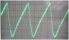
i'm not sure why you're having such severe slewing problems, but it could be that your input transistor is current starved, and can't keep up with charging the compensation cap (or even the miller capacitance of the voltage amplifier transistor). it's late here, so i'll take a fresh look at it tomorrow.
 
Last edited:
next time you take a pic of the spectrum analyzer display, turn off the flash.

Sorry, it wasnt the flash, it was the light from the ceiling.

I took 2 pics of the same THD measurement...........................

The 2nd pic seems to be clearer:D, the values ie. Still got some reflection there thou:D.
 

Attachments

  • clearer thd..PNG
    clearer thd..PNG
    527.4 KB · Views: 288
Status
Not open for further replies.

Latest threads

New Articles From Microcontroller Tips

Back
Top