Hi again,
An absolute value circuit is not exactly just a full wave rectifier bridge made of only diodes, it's a op amp circuit that is a little more accurate for low level signals. A bridge rectifier has diode drops which impairs its ability to function accurately with signals that are comparable to the diode drops. The op amp equivalent circuit is better in that it can rectify lower level signals much more accurately.
Are you saying that you need to have the output go negative when the input goes negative? In that case you also need a circuit to detect the negative portion of the input and switch the output so that it goes negative too (after taking the absolute value and square root).
I'll take a look at your circuit and see what i can find out. What are the two adjustments doing for you?
Also, what range input are you looking for?
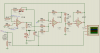
That circuit looks a little strange. Did you check it for numerical accuracy?
Basic tests:
When you input 0.25v, did you get 0.5v out?
When you input 1v, did you get 1v out?
When you input 4v, did you get 2v out?
When you input 9v, did you get 3v out?
I ask because certain parts of the circuit look very unorthodox (R2 for example).
They make pretty good multiplier chips these days i think so you may be better off with a design based on a multiplier chip.
You can also consider using a micro controller chip with built in AD converter and DA output.
Thank you very much MrAl,
To the second circuit I agreed that It is a bit strange (the Link of my above Post explains how it works But I am not able to understand it..).
I tried the circuit for voltages of one and bigger than 1 in the simulator, and it actually works. The link says that the first stage is a squarer but i don't know how they take the square root by a squarer circuit!
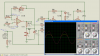
As I told I made the above circuit practically but It did not work in practice!!
Now I want to back to the first circuit and make it practically to see the results.
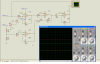
One question which I have is that I do not now what is the functioning of "U7: D" here in the circuit (Plz take a look at the below pic)?
The disner says that it acts to give an offset to the circuit and to normalize the signal. I can not understand why they need it and why they used such a circuitry to generate an offset? Why they put a diode in the feedback loop of U7: D to generate a DC offset? Why they do not use a normal voltage divider?! (the explanations regarding the circuit are here:
https://docs.google.com/viewer?a=v&...qHUkjw&sig=AHIEtbR-h2_IX6byp-m6pXdFE1zgXr91zQ ( pLz take a look at "D.2.2" and "D.4")).
I want to remove he D7: D somehow and use its op-amp in the output so that give the input a 180 degrees phase shift so that I could give positive signals to the input (if you tak a look at the below pic you'll notice that it accepts the just negative inputs not positive ones).
MrAl can you give me a view of D7:d stage please?
thanks
Edited...
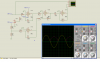
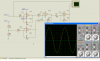
Ok here's the results of this circuit in practice while the input peak is almost 2V:
So the original circuit using 4 op-amps as "log -> x0.5 -> antilog" works in practice.
I have to perform some trims on it to get the best results.
Any idea plz?