Continue to Site

Welcome to our site!

Electro Tech is an online community (with over 170,000 members) who enjoy talking about and building electronic circuits, projects and gadgets. To participate you need to register. Registration is free. Click here to register now.

  • Welcome to our site! Electro Tech is an online community (with over 170,000 members) who enjoy talking about and building electronic circuits, projects and gadgets. To participate you need to register. Registration is free. Click here to register now.

AD-501-B (w/ LC7932M LED driver ICs) 16x32 LED Display questions

Status
Not open for further replies.

tdg8934

New Member
I purchased this serial interfaced 16x32 LED display board here (#5):
https://www.futurlec.com/Specials.shtml

Even though the datasheet (attached) is in THAI (yes - it's a challenge), I have been able to get the board interfaced to a Parallax SX-28 (similar to a PIC chip) using their SX/B (Basic language). I have also attached the SX/B program to examine. I have also written similar code for a Parallax Basic Stamp II (attached).

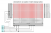
However, the display board is designed to have the 16 rows and 2 sets of 16 columns controlled by 3 LC7932M LED driver ICs and some FETs, AND they are all tied to the same /STROBE, /LATCH and CLOCK signals. See page 2 of the datasheet (THAI) to clarify this.

Since these signals are tied together, I can't really use an interrupt on the 16 rows so all I can do is scan the rows while feeding in data into the 2 sets of 16 columns. It flickers some when doing this and I wanted to know if I am missing something here or if there is a better way to do this.

Any help would be appreciated.

Thanks.
 

Attachments

  • AD501B.ZIP
    361.6 KB · Views: 1,006
They're using a simple method for loading the shift registers with 48 bits of data using only 16 clock pulses. I use a similar method for loading 56 bits of data into seven 8-bit MIC5821 shift registers or 64 bits of data into eight 8-bit MIC5821 shift registers using only 8 clock pulses on my display subsystem designs.

You simply need to 'clock' bit 15 for all three shift registers at the same time, followed by bit 14 for all three shift registers, and so on through bit 0 for all three shift registers, then 'strobe' the shift registers onto the outputs to update the display.

Mike
 
Hello Mike. How are you? Somehow I thought you might answer my question. That's great!

What I am doing as seen in mainly in the "CheckDataSin" routine in the "16x32LED_v6.sxb" program, (view it in notepad or something)...is pretty much what you are saying.

First the 2 sets of 16 bits of column data and 16 bits of row data (top row) are sent to the 3 shift registers. Then it all gets latched and strobed out. The process gets repeated 16 times for the 16 rows (top going to the bottom) and the next 2 sets of column data - in the Main: loop of the program.

So it appears that I am doing this correct. Is this right?
 
I'm fine, thank you Sir. I trust you and family are well and enjoying this wonderful summer season?

Haven't looked at your code. Sorry.

The placement of the transistor drivers on the rows in that schematic suggests they're "scanning" rows (here we go again, grin). That means your 16 bit "row" variable is just a Johnson type ring counter (only 1 bit low or high depending on the polarity you need to drive the row transistors) and you should be turning on only one row at a time while 'real' LED data is latched in the two 16 bit column drivers.
 
Mike,

My 18 year old son from my first marriage is now living with us permanently so we are all happy about that. Thanks for asking.

As far as the display goes... the code sets the rows to be only on 1 row at a time as you stated.

The row is controlled by the "data1" variable which changes rows by shifting it by 2 (e.g. top row means data1 = 1, 2nd row means data1 = 2, 3rd row means data1 = 4....the 16th row means data1 = 65535. ).

One time I did try to scan the rows from the bottom to the top (e.g. 65535, 32768, etc...8,4,2,1) but it did not work in that all of the rows above the one I was setting would all light up both sets of columns fully (regardless of what data was set in both sets of columns). Hopefully you followed that.

So from what I understand, I am doing this correctly.

If this is the case how do I effectly do anything with this?

Thanks.
 
If this is the case how do I effectly do anything with this?
Well, there are probably several different ways to manage display data. I would typically use a 64 byte "display buffer" for 512 LEDs which is manipulated by MAIN and my ISR driver would pull data from that buffer to drive the displays as a background task.

I suppose you could have a whole bunch of the these 64 byte display buffer "frames" in a large external I2C eeprom for animation or such if you don't want to manipulate display bit data manually in a single 64 byte display buffer.
 
I wonder if your flicker problem might be caused by the way you're driving the LC7932M 'latch' and 'strobe' inputs? Ideally you would like to load the shift registers and then transfer that data onto the outputs without flicker but I haven't quite figured out the correct sequence for the 'latch' and 'strobe' signals from the data sheet.
 
Thanks for the info Mike.

The minor flickering I thought was due to it being in a repeating loop in the MAIN: routine - also that it has 16 rows (not the smaller 8) to scan. But I don't know for sure. Brightness is pretty good.

Since the program is in a Basic like language (SX/B), I will probably just make multiple WDATA statements (16 bit word DATA) and try to feed them in one after the other to get some scrolling from the top to bottom.

I will let you know my progress in a day or so.

Thanks!
 
Well...I have come to realize that this module is probably more trouble that it's worth. Since the row (CLOCK, /LATCH and /STROBE) lines are all tied together for the 16 row LC7932M LED driver IC (AND) the 2 sets of 16 column LC7932M LED driver ICs....all I can do is turn on one row at a time (top to bottom) whenever a column set is on.

With WDATA statements, I can pretty much display items such as a pyramid, upside down pyramid and the letters EF. (see the WDATA statements to see this). They are repeat displayed for 20 frames then the next display comes on for 20 more frames. The process repeats in a loop. This is the reason for the flickering.

See attached test file.


' =========================================================================
'
' File...... 16x32LED_v6TEST.SXB
' Purpose... SX/B interface to AD-501-B
' Author.... Timothy Gilmore (Special help and thanks to JonnyMac)
' E-mail.... gilmoret@us.saic.com
' Started... 03 JUN 2007
' Updated... 01 JUL 2007
'
' =========================================================================


' -------------------------------------------------------------------------
' Program Description
' -------------------------------------------------------------------------
' BS2 conversion program to SX-28 interface with an AD-501-B

' -------------------------------------------------------------------------
' Device Settings
' -------------------------------------------------------------------------

DEVICE SX28, OSC4MHZ, TURBO, STACKX, OPTIONX 'Use no external resonator
'DEVICE SX28, OSCHS3, TURBO, STACKX, OPTIONX 'Use external 20 MHz resonator
FREQ 4_000_000
'FREQ 20_000_000
ID "AD-501-B"


' -------------------------------------------------------------------------
' IO Pins
' -------------------------------------------------------------------------

SIN_1 PIN RB.0
SIN_2 PIN RB.1
SIN_3 PIN RB.2
CLOCK PIN RB.3
LATCH PIN RB.4
STROBE PIN RB.5

' -------------------------------------------------------------------------
' Constants
' -------------------------------------------------------------------------

Delay CON 1 ' Set the Forward Delay time

' -------------------------------------------------------------------------
' Variables
' -------------------------------------------------------------------------

data1 VAR Word
data2 VAR Word
data3 VAR Word

tmpW1 VAR Word
tmpW2 VAR Word

result VAR Word

tmpB1 VAR Byte
tmpB2 VAR Byte

I VAR Byte
J VAR Byte

value VAR Byte

K VAR Byte


'dat2 dat3
'SIN_2 SIN_3
'xxxxxxxxxxxxxxxx xxxxxxxxxxxxxxxx | SIN_1 data1
'0xxxxxxxxxxxxxxx xxxxxxxxxxxxxxx0 | |
'00xxxxxxxxxxxxxx xxxxxxxxxxxxxx00 v |
'000xxxxxxxxxxxxx xxxxxxxxxxxxx000 v
'0000xxxxxxxxxxxx xxxxxxxxxxxx0000 |
'00000xxxxxxxxxxx xxxxxxxxxxx00000 |
'000000xxxxxxxxxx xxxxxxxxxx000000 v
'0000000xxxxxxxxx xxxxxxxxx0000000 on/off x-rows
'00000000xxxxxxxx xxxxxxxx00000000
'000000000xxxxxxx xxxxxxx000000000 |
'0000000000xxxxxx xxxxxx0000000000 |
'00000000000xxxxx xxxxx00000000000 |
'000000000000xxxx xxxx000000000000 |
'0000000000000xxx xxx0000000000000 v
'00000000000000xx xx00000000000000
'000000000000000x x000000000000000

'dat2b dat3b
'SIN_2 SIN_3
'000000000000000x x000000000000000 | SIN_1 data1
'00000000000000xx xx00000000000000 | |
'0000000000000xxx xxx0000000000000 v |
'000000000000xxxx xxxx000000000000 v
'00000000000xxxxx xxxxx00000000000 |
'0000000000xxxxxx xxxxxx0000000000 |
'000000000xxxxxxx xxxxxxx000000000 v
'00000000xxxxxxxx xxxxxxxx00000000 on/off x-rows
'0000000xxxxxxxxx xxxxxxxxx0000000
'000000xxxxxxxxxx xxxxxxxxxx000000 |
'00000xxxxxxxxxxx xxxxxxxxxxx00000 |
'0000xxxxxxxxxxxx xxxxxxxxxxxx0000 |
'000xxxxxxxxxxxxx xxxxxxxxxxxxx000 |
'00xxxxxxxxxxxxxx xxxxxxxxxxxxxx00 v
'0xxxxxxxxxxxxxxx xxxxxxxxxxxxxxx0
'xxxxxxxxxxxxxxxx xxxxxxxxxxxxxxxx


' -------------------------------------------------------------------------
' INTERRUPT 3000
' -------------------------------------------------------------------------

'ISR_Start:

'ISR_Exit:
' RETURNINT


' =========================================================================
PROGRAM Start
' =========================================================================

' -------------------------------------------------------------------------
' Subroutine Declarations
' -------------------------------------------------------------------------

CheckDataSin SUB

BITVAL FUNC 1, 2, 3 'Thanks to JonnyMac for these cool functions!
'It saved me alot of coding.

WREAD FUNC 2, 3 ' read word from WDATA

' -------------------------------------------------------------------------
' Program Code
' -------------------------------------------------------------------------


Start:
' initialization code here

LOW SIN_1 'SIN_1 is off
LOW SIN_2 'SIN_2 is off
LOW SIN_3 'SIN_3 is off

HIGH STROBE 'STROBE is off
HIGH LATCH 'LATCH is off
LOW CLOCK 'CLOCK is off (Active high)

Main:
FOR K = 1 to 20
data1 = 1 'Start from the top row (for first pattern)
FOR J = 0 TO 15
data2 = WREAD dat2, J
data3 = WREAD dat3, J
CheckDataSin
NEXT
NEXT

FOR K = 1 to 20
data1 = 1 'Start from the top row (for next pattern)
FOR J = 0 TO 15
data2 = WREAD dat2b, J
data3 = WREAD dat3b, J
CheckDataSin
NEXT
NEXT

FOR K = 1 TO 20
data1 = 1 'Start from the top row (for next pattern)
FOR J = 0 TO 15
data2 = WREAD dat2c, J
data3 = WREAD dat3c, J
CheckDataSin
NEXT
NEXT

GOTO Main

End


' -------------------------------------------------------------------------
' Subroutine Code
' -------------------------------------------------------------------------


' Use: result = WREAD table, element
' -- "table" is a WDATA table
' -- "element" is the nth word in the WDATA table

FUNC WREAD
tmpW1 = __WPARAM12 ' get table address
tmpB1 = __PARAM3 ' get element
tmpB1 = tmpB1 << 1 ' x2; convert to LSB offset
tmpW1 = tmpW1 + tmpB1 ' add offset to address
READ tmpW1, tmpW2_LSB, tmpW2_MSB
RETURN tmpW2
ENDFUNC


' Use: value = BITVAL someVal, position
' -- "someVal" can be a byte or word

FUNC BITVAL
IF __PARAMCNT = 2 THEN ' byte passed?
tmpW1 = __PARAM1 ' get byte value
tmpB1 = __PARAM2 ' get bit position
ELSE ' word passed
tmpW1 = __WPARAM12 ' word was passed
tmpB1 = __PARAM3 ' get bit position
ENDIF
tmpB2 = 0 ' assume cleared
IF tmpB1 >= 0 THEN ' position value legal?
IF tmpB1 <= 15 THEN
tmpW2 = 1 << tmpB1 ' create bit mask
tmpW2 = tmpW2 & tmpW1 ' clear other bits
IF tmpW2 > 0 THEN ' if not zero
tmpB2 = 1 ' bit was 1
ENDIF
ENDIF
ENDIF
RETURN tmpB2
ENDFUNC


CheckDataSin:
For I = 0 to 15

value = BITVAL data1, I

IF value = 1 THEN
HIGH SIN_1
ELSE
LOW SIN_1
ENDIF

value = BITVAL data2, I

IF value = 1 THEN
HIGH SIN_2
ELSE
LOW SIN_2
ENDIF

value = BITVAL data3, I

IF value = 1 THEN
HIGH SIN_3
ELSE
LOW SIN_3
ENDIF

HIGH CLOCK
LOW CLOCK

NEXT

LOW LATCH 'LATCH is on
HIGH LATCH 'LATCH is off

LOW STROBE 'STROBE is on
PAUSE Delay
HIGH STROBE 'STROBE is off

data1 = data1 << 1 'SIN_1 data is shifted from top row to bottom row

RETURN


' =========================================================================
' User Data
' =========================================================================

'Pgm_ID:
' DATA "SX/B 1.51 Template", 0

dat2:
WDATA %1111111111111111
WDATA %0111111111111111
WDATA %0011111111111111
WDATA %0001111111111111
WDATA %0000111111111111
WDATA %0000011111111111
WDATA %0000001111111111
WDATA %0000000111111111
WDATA %0000000011111111
WDATA %0000000001111111
WDATA %0000000000111111
WDATA %0000000000011111
WDATA %0000000000001111
WDATA %0000000000000111
WDATA %0000000000000011
WDATA %0000000000000001

dat3:
WDATA %1111111111111111
WDATA %1111111111111110
WDATA %1111111111111100
WDATA %1111111111111000
WDATA %1111111111110000
WDATA %1111111111100000
WDATA %1111111111000000
WDATA %1111111110000000
WDATA %1111111100000000
WDATA %1111111000000000
WDATA %1111110000000000
WDATA %1111100000000000
WDATA %1111000000000000
WDATA %1110000000000000
WDATA %1100000000000000
WDATA %1000000000000000


dat2b:
WDATA %0000000000000001
WDATA %0000000000000011
WDATA %0000000000000111
WDATA %0000000000001111
WDATA %0000000000011111
WDATA %0000000000111111
WDATA %0000000001111111
WDATA %0000000011111111
WDATA %0000000111111111
WDATA %0000001111111111
WDATA %0000011111111111
WDATA %0000111111111111
WDATA %0001111111111111
WDATA %0011111111111111
WDATA %0111111111111111
WDATA %1111111111111111

dat3b:
WDATA %1000000000000000
WDATA %1100000000000000
WDATA %1110000000000000
WDATA %1111000000000000
WDATA %1111100000000000
WDATA %1111110000000000
WDATA %1111111000000000
WDATA %1111111100000000
WDATA %1111111110000000
WDATA %1111111111000000
WDATA %1111111111100000
WDATA %1111111111110000
WDATA %1111111111111000
WDATA %1111111111111100
WDATA %1111111111111110
WDATA %1111111111111111

dat2c:
WDATA %0000000000000000
WDATA %0111111111111111
WDATA %0111100000001111
WDATA %0111100000000000
WDATA %0111100011110000
WDATA %0111111111110000
WDATA %0111100011110000
WDATA %0111100000000000
WDATA %0111100000001111
WDATA %0111111111111111
WDATA %0000000000000000

dat3c:
WDATA %0000000000000000
WDATA %0111111111111111
WDATA %0111100000001111
WDATA %0111100000000000
WDATA %0111100011110000
WDATA %0111111111110000
WDATA %0111100011110000
WDATA %0111100000000000
WDATA %0111111000000000
WDATA %0000000000000000
 
Last edited:
The problem is probably the BASIC Stamp. It's just not very powerful or fast. Try a compiler like PIC BASIC, Great Cow BASIC, C or assembler, lots of speed and much faster than the BASIC Stamp.
 
I wonder if you're giving up too easily? But I doubt I can be of much help since we speak different languages and mcu's (grin).

(1) Use an interrupt driver to paint the display hardware from a 64 byte (512 bit) "display" buffer. I would throw 16 special "shift register" formatted bytes onto the bus each interrupt and then configure the 16 special "shift register" bytes from the "display buffer" for the next interrupt cycle (the next row).

(2) Design a "character generator" that will place a graphic character from your graphic character set tables anywhere in the "display" buffer at position 'HPOS' & 'VPOS'. I used a character generator like this to "paint" characters and graphics into the video RAM in the EPG and EPG II (earliest versions of the current TV Guide Channel, circa 1984).

Example; setup HPOS and VPOS, tell the character generator which character set table to use, then send the character generator a string of characters ("AAaa442y"). Each character in that string would be mapped to an 8x8 character bit pattern or an 8x8 graphic pattern in a character table. As the character generator places the bit pattern for each character into the "display buffer" it auto increments HPOS for the next character.
----------------------------------------------
Here's an interrupt driver for an 8x56 display (scanning columns again, sorry). I'm sure it's gonna seem completely alien to you but what the heck, maybe it'll help. The display is drawn vertically to show the bus/interface connections but it's actually a horizontal display.

Code:
;******************************************************************
;
COLUMN  equ     h'20'           ; column number (0..7)
COLPOS  equ     h'21'           ; column ring counter (00000001)
;
SBuff   equ     h'38'           ; scan buffer 30..37,  8 bytes
DBuff   equ     h'40'           ; disp buffer 40..77, 56 bytes
WBuff   equ     h'78'           ; work buffer 78..7E,  7 bytes

        radix   dec

;******************************************************************
;
;  K8LH High Performance 9-pin Display Subsystem ISR Driver
;
;  This subsystem hardware/software design supports from one
;  to seven 8x8 display modules.
;
;  One LED column in each of the seven 8x8 modules is driven
;  during each 1.0-msec interrupt cycle for an overall 12.5%
;  duty cycle and 125-Hz refresh rate.
;
;  A minimum PWM 'on-time' of 1% provides a 10-usec window
;  at the start of each interrupt cycle where the PWM signal
;  drives the MIC5821 Output Enable lines high (display off)
;  which allows me to use the RB7-RB0 column driver lines
;  temporarily as MIC5821 <DAT> and <CLK> lines to load the
;  seven MIC5821 shift registers.
;
;  Serial data is clocked into seven MIC5821 shift registers
;  in parallel by stuffing PORTB with eight data bytes, each
;  containing <DAT> bits in b7 through b1 and a <CLK> bit in
;  b0 which is preset to '0'.
;
;  The 1% minimum PWM 'on' time limits maximum brightness to
;  99% but the 1% loss of brightness is inperceivable at the
;  high end.
;
;  24 cycles, 4.8-usecs (20-MHz clock)
;
ISR_load_shift_registers

        movff   SBuff+7,LATB    ; bit 7 byte [ddddddd0]
        bsf     LATB,0          ; clock data [ddddddd1]
        movff   SBuff+6,LATB    ; bit 6 byte
        bsf     LATB,0          ;
        movff   SBuff+5,LATB    ; bit 5 byte
        bsf     LATB,0          ;
        movff   SBuff+4,LATB    ; bit 4 byte
        bsf     LATB,0          ;
        movff   SBuff+3,LATB    ; bit 3 byte
        bsf     LATB,0          ;
        movff   SBuff+2,LATB    ; bit 2 byte
        bsf     LATB,0          ;
        movff   SBuff+1,LATB    ; bit 1 byte
        bsf     LATB,0          ;
        movff   SBuff+0,LATB    ; bit 0 byte
        bsf     LATB,0          ;
;
;  resume PORTB column driver duties before PWM goes low and
;  advance the column ring counter for the next cycle
;
;  3 cycles, 0.6-usecs
;
        comf    COLPOS,W        ; invert bits (only 1 bit low)
        movwf   LATB            ; setup PORTB column drivers
        rlncf   COLPOS,F        ; advance column ring counter


;******************************************************************
;
;  build the eight '5821 shift register bytes in SBuff for the
;  next interrupt cycle.  first copy the correct seven display
;  buffer bytes for the next interrupt cycle and put them into
;  the WBuff work buffer.  then combine all of the b7 bits, b6
;  bits, b5 bits, etc., into their own bytes in the eight byte
;  SBuff shift register data buffer.
;
;  step <1>
;  copy 7 display column data bytes into the WBuff work buffer
;
;  25 cycles, 5.0-usecs
;
ISR_Display_Prep

        lfsr    0,DBuff         ; FSR0 = address DBuff[0,0]
        incf    COLUMN,F        ; Column++
        bcf     COLUMN,3        ; Column %= 8
        movf    COLUMN,W        ; WREG = Column (0..7)
        movff   PLUSW0,WBuff+0  ; WBuff[0] = DBuff[0,Column]
        addlw   8               ;
        movff   PLUSW0,WBuff+1  ; WBuff[1] = DBuff[1,Column]
        addlw   8               ;
        movff   PLUSW0,WBuff+2  ; WBuff[2] = DBuff[2,Column]
        addlw   8               ;
        movff   PLUSW0,WBuff+3  ; WBuff[3] = DBuff[3,Column]
        addlw   8               ;
        movff   PLUSW0,WBuff+4  ; WBuff[4] = DBuff[4,Column]
        addlw   8               ;
        movff   PLUSW0,WBuff+5  ; WBuff[5] = DBuff[5,Column]
        addlw   8               ;
        movff   PLUSW0,WBuff+6  ; WBuff[6] = DBuff[6,Column]
;
;  step <2>
;  build SBuff for next display interrupt cycle.  all of the
;  b0 bits in one byte, b1 bits in the next byte, and so on.
;  bit 0 in each byte is preset to '0' to drive the CLK line
;  low on the seven MIC5821 drivers as each byte is written
;  to PORTB in the ISR_load_shift_registers routine.
;
;  145 cycles, 29.0-usecs
;
        lfsr    0,SBuff         ; shift register buffer address
V1      clrf    INDF0           ; for (n=0; n<8; ++n)
        rrcf    WBuff+0,F       ;   WBuff[0] >>= 1
        rrcf    INDF0,F         ;   SBuff[n] >>= 1 + C*128
        rrcf    WBuff+1,F       ;   WBuff[1] >>= 1
        rrcf    INDF0,F         ;   SBuff[n] >>= 1 + C*128
        rrcf    WBuff+2,F       ;   WBuff[2] >>= 1
        rrcf    INDF0,F         ;   SBuff[n] >>= 1 + C*128
        rrcf    WBuff+3,F       ;   WBuff[3] >>= 1
        rrcf    INDF0,F         ;   SBuff[n] >>= 1 + C*128
        rrcf    WBuff+4,F       ;   WBuff[4] >>= 1
        rrcf    INDF0,F         ;   SBuff[n] >>= 1 + C*128
        rrcf    WBuff+5,F       ;   WBuff[5] >>= 1
        rrcf    INDF0,F         ;   SBuff[n] >>= 1 + C*128
        rrcf    WBuff+6,F       ;   WBuff[6] >>= 1
        rrcf    POSTINC0,F      ;   SBuff[n] >>= 1 + C*128
        btfsc   FSR0L,3         ;
        bra     V1              ;
matrix-7x8x8-png.13422
 
Last edited:
Tim,

Forget that previous example. It's way off base. Can't use PWM on that 16x32 board and you're scanning rows not columns.

I did however put together a PIC driver for that ($12.90) 16x32 matrix display just for giggles and I'd be happy to pass it along if you or someone else on the forum asks. I'll work on character generator code next.

Mike
 
Last edited:
Mike,

I had almost given up on this headache. I would love to see what you have for this IF YOU HAVE IT ALREADY. Don't spend the time unless it's ready or close so you dont waste your time.

Thanks again Mike!
 
This is my second version of a simple PIC ISR driver for your OEM 16x32 matrix display board. I didn't have the board schematic or the driver data sheets with me when I wrote this code so I may have the bit pattern backwards. I believe from the documentation that the STB signal is an active low output enable (this display may be a good candidate for PWM brightness control).

Mike

Code:
;******************************************************************
;
DBuff   equ     h'00'           ; disp buffer 00..3F, 64 bytes
WBuff   equ     h'80'           ; work buffer 80..85, 6 bytes

RowPos  equ     h'86'           ; ISR, 16 bit row ring counter
Row     equ     h'88'           ; ISR, row number (0..15)
Counter equ     h'89'           ; ISR, counter

;******************************************************************

        radix   dec

;******************************************************************
;
;  K8LH Experimental 16x32 6-pin Display Subsystem ISR Driver
;
;  This subsystem driver was designed for an OEM 16x32 display
;  that uses three 16 bit serial-to-parallel driver IC's.
;
;  One 32 LED row is driven each 1.0-msec interrupt cycle for
;  an overall 6.25% duty cycle and 62.5-Hz refresh rate.
;
;  Serial data is clocked into three 16 bit shift registers
;  in parallel by stuffing PORTB with 16 data bytes, each
;  containing <DAT> bits in b0, b1, and b2, a <CLK> bit in b3
;  which is preset to '0', and a <LAT> bit in b4 which is
;  preset to '1'.  This driver loads the shift registers with
;  bit 15 data first.
;
;       RB0 = DAT line on row driver IC
;       RB1 = DAT line on 1st column driver IC
;       RB2 = DAT line on 2nd column driver IC
;       RB3 = CLK line on all 3 ICs
;       RB4 = LAT line on all 3 ICs
;       RB5 = STB line on all 3 ICs
;
;  263 cycles, 52.6 usecs, 5.26% "overhead" (20 MHz clock)
;              33.2 usecs, 3.32% "overhead" (32 MHz clock)
;
ISR_load_shift_registers

        clrf    FSR1H           ;
        rlncf   Row,W           ; row number (0..15) x4
        rlncf   WREG,W          ;
        movwf   FSR1L           ; FSR1 = DBuff(Row).byte(0)
        movff   POSTINC1,WBuff+0    ; b07..b00 display data
        movff   POSTINC1,WBuff+1    ; b15..b08 display data
        movff   POSTINC1,WBuff+2    ; b23..b16 display data
        movff   POSTINC1,WBuff+3    ; b31..b24 display data
        movff   RowPos+0,WBuff+4    ; b07..b00 ring counter
        movff   RowPos+1,WBuff+5    ; b15..b08 ring counter
        bsf     Counter,4       ; Cntr = 16
v0      movlw   b'00000010'     ; preload WREG
        rlcf    WBuff+0,F       ; rlcf lo byte, DBuff(Row,0)
        rlcf    WBuff+1,F       ; rlcf hi byte, DBuff(Row,1)
        rlcf    WREG,F          ; pick up b2 (2nd column SR)
        rlcf    WBuff+2,F       ; rlcf lo byte, DBuff(Row,2)
        rlcf    WBuff+3,F       ; rlcf hi byte, DBuff(Row,3)
        rlcf    WREG,F          ; pick up b1 (1st column SR)
        rlcf    WBuff+4,F       ; rlcf lo byte, RowPos
        rlcf    WBuff+5,F       ; rlcf hi byte, RowPos
        rlcf    WREG,F          ; pick up b0 (row SR)
        movwf   LATB            ; update port, [--010ddd]
        bsf     LATB,3          ; toggle <CLK> [--011ddd]
        decfsz  Counter,F       ; all 16 iterations?
        bra     v0              ; no, branch, else
        bcf     LATB,4          ; toggle <LAT> [--001ddd]
        bsf     LATB,4          ; tobble <LAT> [--011ddd]
;
;  advance Row variable and RowPos ring counter for next cycle
;
        incf    Row,F           ; Row++
        bcf     Row,4           ; Row % 16 (well, sort of)
        rrcf    RowPos+0,W      ; rrcf lo byte into W to save C
        rrcf    RowPos+1,F      ; rrcf hi byte
        rrcf    RowPos+0,F      ; rrcf lo byte
        retfie  FAST            ;

;******************************************************************
;
Init_display

        lfsr    0,DBuff         ; clear display buffer & vars
iloop   clrf    POSTINC0        ;
        movf    FSR0L,W         ;
        xorlw   0xC0            ; 00..BF cleared?
        bnz     iloop           ; no, branch, else
        clrf    RowPos          ; setup RowPos ring counter
        clrf    RowPos+1        ;
        bsf     RowPos+1,7      ; RowPos = %1000000000000000
        movlw   b'00010000'     ;
        movwf   PORTB           ; set LAT (B4) pin hi
        clrf    TRISB           ; PORTB all outputs
        return                  ;
 

Attachments

  • Matrix 16x32 OEM.PNG
    Matrix 16x32 OEM.PNG
    35.5 KB · Views: 3,663
Last edited:
Tim,

I've got those pdf files now and I've looked at your code a little closer. Looks like CLK is active high, LAT is active low, and STB is actually an active low Output Enable (hardware will support PWM brightness control, cool).

Also looks like I've got all of the bit patterns backwards. I'll modify my PIC driver.

If you can dimension an array as 32 bit long word you could map the entire 64 byte display buffer to a 16 element array. That would allow you to modify any row by assigning a new value to it's corresponding array element. Your compiler would hopefully translate that array element assignment into just a few instructions that copy the 4-byte/32-bit argument directly into the display buffer. Of course the display driver would handle the buffer-to-hardware process in the background.

Code:
DIM Display(16) as LongWord


Display(15) =  %00000000000000000000000000000000
Display(14) =  %01111111111111110000000000000000
Display(13) =  %01111111111111110000000000000000
Display(12) =  %01111000000011110000000000000000
Display(11) =  %01111000000011110000000000000000
Display(10) =  %01111000000000000000000000000000
Display(9)  =  %01111000111100000000000000000000
Display(8)  =  %01111111111100000000000000000000
Display(7)  =  %01111111111100000000000000000000
Display(6)  =  %01111000111100000000000000000000
Display(5)  =  %01111000000000000000000000000000
Display(4)  =  %01111000000011110000000000000000
Display(3)  =  %01111000000011110000000000000000
Display(2)  =  %01111111111111110000000000000000
Display(1)  =  %01111111111111110000000000000000
Display(0)  =  %00000000000000000000000000000000
PAUSE Delay
Can I confirm the "row" pattern is active low ('1111111111111110') ?
 
Last edited:
Mike,

The row is an active high but set to move from the top row to the next lower row when it equals the following:

data1 = data1 << 1 {This is the code use to shift the bits left}

data1 = 1 (2^0) when on the 1st / top row or (data1 = 0000000000000000)
data1 = 2 (2^1) when on the 2nd row or (data1 = 0000000000000001)
data1 = 4 (2^2) when on the 3rd row or (data1 = 0000000000000010)
data1 = 8 (2^3) when on the 4th row or (data1 = 0000000000000100)
.
.
.
data1 = 32768 (2^15) when on the 16th row or (data1 = 1000000000000000)

This is where I beleive the problem is in that I can only have the row assignments set to 1 bit (or row on) at any time with a corresponding set column of 16 bits each for data2 and data3 ..... because the lines are all tied together.

I'm interested in what you have found and let me know...

Thanks!
 
Ah, those are sinking drivers. Input data is inverted on the outputs. Duh!

Are you sure those bit patterns aren't like this?

0000000000000001 top row
0000000000000010 2nd row
0000000000000100 3rd row
~~~~~
1000000000000000 bottom row

Are you shifting 'row' data least significant bit first? For example, when you send it %0000000000000001, are you activating the top most row of the display which the schematic shows as bit 15/output 15 on the 'row' shift register?
 
Mike,

YES YOU ARE CORRECT. MY MISTAKE!!!

I did another check and set data1=1 and only the top line had column data (data2 and data3) displayed.

When I set it to data1=32768 then the bottom row turned column data on.

If I set it to data1 = 0 then nothing is displayed.

If I set it to data1 = 3 then the top 2 rows displayed column data as you would think.

And by setting data1=32767 then the first 15 rows display data.

data1=1 is the top row because all of the PCB labeling on the reverse side (IC's and components) are listed upright for reference.

Let me know if there is anything else you need. I am awaiting your feedback.

Thanks!
 
Their schematic shows the top row of the matrix corresponds to the bit 15 shift register input. The '7932 Data Sheet seems to imply that the first of sixteen bits shifted into the shift register is bit 15, the most significant bit.

Are you shifting that %0000000000000001 'row' value into the 'row' driver least significant bit first? Put another way, are you representing your values, for example %0000000000000001, in reverse order, least significant bit on the left and most significant bit on the right?
 
Mike,

The "data1 = data1 << 1" statement shifts the data1 variable from 1 to 32768.

Should I change this to shift the other way (meaning from the bottom to the top). Does it matter? I can simply turn the display upside down?

I did try this once when I initially set "data1 = 32768" and then set "data1 = data1 >> 1" but it would start at the bottom row and move towards the top BUT all of the rows from the bottom to the top STAYED ON. It's a little hard to explain but maybe I set it up wrong. I just found that the way I scroll the row from top to bottom seems to work well.
 
Status
Not open for further replies.

Latest threads

New Articles From Microcontroller Tips

Back
Top