Electro Tech is an online community (with over 170,000 members) who enjoy talking about and building electronic circuits, projects and gadgets. To participate you need to register. Registration is free. Click here to register now.
Welcome to our site! Electro Tech is an online community (with over 170,000 members) who enjoy talking about and building electronic circuits, projects and gadgets. To participate you need to register. Registration is free. Click here to register now.
can't figure it out though ¬_¬ should be able to, surely..
looking on Texas Instruments, the control signal and/or volt is pin 1, with pin 14 as the power for the chip.. fine.. so i connect that to my power source.. pin 2 is the other part of the gate which goes to a resisitor looking around, 100k, which then goes to a capactor (2.2uf) and then to ground. the other end of the resisitor is connected to pin 3, the output of the NAND gate, which is then the signal line.
Connect pins 1 & 2 together, with a capacitor to ground.
Connect a moderate value resistor from one side of the switch to power and ground the other side of the switch; eg. 1K.
Connect another resistor from the switch terminal with that resistor, to the gate input / capacitor; eg. 1K or anything up to 100K.
10K would be reasonable with a 10uF cap on the gate input.
The gate output will go high a short time after the switch is pressed and low a short time after it is released.
okay.. sorry about this.. somehow getting it wrong... got pin 1 &2 connected together, to a 2,2uf capacitor (cause I had it to hand) then to ground.. got a 1k resisitor going from power to one side of switch. other side of switch is going to ground and to 10k resisitor, which is going to 10uf cap and then to pin1 (as pin 1 and 2 are the inputs). pins4&5, 7, 8&9, 11&12 are all going to ground. pin 14 is power, pin 3 is output so that goes to the main circuit .
You need to swap the two resistors. The pullup resistor (going to +Vdd) needs to be a much higher value than the switched resistor going to ground.
For the CD4093, you should have connected to pins 1 and 2:
- R1 (10k or greater) going to +Vdd
- C1 the positive terminal of a 2.2uF capacitor. The negative terminal to gnd
- R2 a 1K resistor, the other end of which connects to your switch. The other side of the switch goes to gnd.
The output of the debounced signal will be on pin 3.
Of course, the power pins of the CD4093 need to be connected to the power source. And there should be a decoupling capacitor across the the power pins as close as possible to the CD4093 as possible. Anything from about .01uF to 1uF will work.
And all unused inputs of the CD4093 must be tied to either gnd or
Get EasyEDA from JLCPCB.com . It's free board layout software. Then you'll be able to make a clear schematic in a couple minutes. It really is easy to learn and use.
This is your schematic, according to the sketch in post #46. There are a number of things wrong....
The nice thing about using a schematic capture tool like EasyEDA – the pins are labeled, so it's easy to see what's what without constantly looking back at the data sheet.
The most obvious errors:
C1 should be connected between pin 14 and ground.
Vcc should be connected directly to pin 14.
For sections 2 and 4, instead of connecting both inputs to ground, you have connected an input and output to ground, and left the other input floating. When the chip is marked with the pin functions, this is easy to see.
Here is the corrected version, as suggested by Chris in post #45. A few minor changes. But notice how much easier it is to see the circuit as a schematic than as a bunch of words.
I do use express PCB by some company that wants to charge a small fortune for custom PCBs to the UK.. which is pretty much all the companies I've seen ¬_¬ but as a PCB layout, i don't think it's that great for just showing the circuit and i have the odd issue.. but yep, layouts are much easier.. and i seam to come off as pretty dumb.. ^_^; which I admit I like to toy and play and try things, more then being an expert or anything. I'll try out the changes and get back a bit later
EasyEDA is a full-featured layout program and quite powerful; while it is offered by JLCPCB (where you can get 10 100mm x 100mm boards for $5), they don't hold you hostage to using their services. A click generates Gerber files that any fab house can use to make your boards.
A clear schematic might help you get to a solution faster....and better help because people can see what you're doing.
I do use express PCB by some company that wants to charge a small fortune for custom PCBs to the UK.. which is pretty much all the companies I've seen ¬_¬ but as a PCB layout, i don't think it's that great for just showing the circuit and i have the odd issue.. but yep, layouts are much easier.. and i seam to come off as pretty dumb.. ^_^; which I admit I like to toy and play and try things, more then being an expert or anything. I'll try out the changes and get back a bit later
JLCPCB is remarkably cheap - I use them all the time - the only drawback is the cost of carriage, but it's well worth it for the speed of DHL.
Any reason you're not using the standard debouncing circuit from way back in the link at the beginning of this thread?.
Check fig2 or fig3 - fig3 allows you to accept much faster pulses, but for a button fig2 is fine. I tend to use 2x22K resistors and a 1uF capacitor for buttons.
for some reason, can't get that simpler circuit to work.... however, it appears i got the one working which was said by ChrisP58 and Visitor. so.. yay? appears to be working totally fine. Have to give a few days of testing but.. seams to be fine now... why he hell it was soo bloody hard for me, no clue, but there you go..
Edit - This was after post #46, but I apparently missed the "post" button.
The switch has a resistor to power. The input a cap to ground. another resistor links the two. It's a very common configuration, as one I found on google, below.
It is the configuration I was describing above, a versatile and generic way of debouncing or adding a short delay.
The signal from the switch + pullup resistor can be from other types of source or logic.
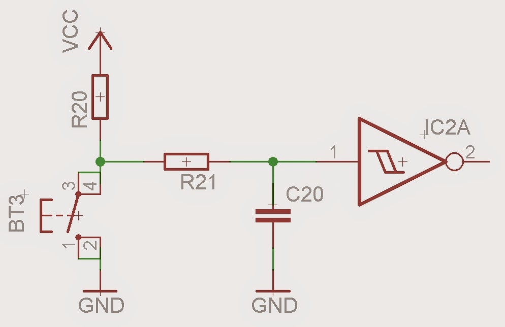
Here's a schematic for Nigel's version. It moves parts around a little, but it's the same number of parts. The R and C values might need some adjustment.
Crossed paths. I guess I didn't follow Chris's description quite right, as it's the same circuit Nigel referenced. A schematic does make things much more clear.
Here's a schematic for Nigel's version. It moves parts around a little, but it's the same number of parts. The R and C values might need some adjustment.
I like this version a little better. Since the two resistors no longer form a voltage divider, their relative value is no longer important, and could be the same value. That makes the BOM for the system simpler.
Here's a schematic for Nigel's version. It moves parts around a little, but it's the same number of parts. The R and C values might need some adjustment.
Well it's hardly my version, it's the standard de-bouncer circuit, as used everywhere. Component wise, as I mentioned previously I use 2 x 22K resistors and a 1uF multilayer ceramic (I have a box of 2000 of them ) for the button inputs, for the pulse counting input I use the same 22K resistors and a much smaller 0.01uF capacitor. The pulse counting part was checked using a function generator, reed relay (to give good bounces), and digital scope - and works to above 2KHz (plenty more than required).
All I was trying to do here was to show that a picture (i.e., schematic) is worth a thousand words, and much easier to understand than a verbal (words as opposed to a picture). Point proven since my schematic based on Chris' description wasn't quite right.
Further, I was attempting to show that using EasyEDA (or similar software) makes life a lot easier because the pin functions are labeled. Based on the OP's hand-drawn schematic, there were significant problems if it was true-to-life: capacitor in series with power to pin 14 and two unused sections of the chip had one input floating and the the other input tied to the output.
I referred to the circuit you introduced as "Nigel's circuit" as a clear concise way of indicating what circuit I was referencing. I suppose I could have said "The debounce circuit developed by Glockenspiel in the late 1500s that Nigel introduced" but it seemed unnecessary. Again, the entire point of my posts in this thread was to show that a clear schematic made exactly what was being discuss clear to everyone involved. A few pictures along the way might have gotten to a solution far sooner than the 3rd page of forum messages.
This site uses cookies to help personalise content, tailor your experience and to keep you logged in if you register.
By continuing to use this site, you are consenting to our use of cookies.

 ) for the button inputs, for the pulse counting input I use the same 22K resistors and a much smaller 0.01uF capacitor. The pulse counting part was checked using a function generator, reed relay (to give good bounces), and digital scope - and works to above 2KHz (plenty more than required).