Continue to Site

Welcome to our site!

Electro Tech is an online community (with over 170,000 members) who enjoy talking about and building electronic circuits, projects and gadgets. To participate you need to register. Registration is free. Click here to register now.

  • Welcome to our site! Electro Tech is an online community (with over 170,000 members) who enjoy talking about and building electronic circuits, projects and gadgets. To participate you need to register. Registration is free. Click here to register now.

Switching Logic Outputs

Status
Not open for further replies.
Why are you placing any external voltage on the switch matrix?
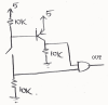
Simply because throughout JoeWawaw's topic he shows that he has 5Volt attached via 100ohm resistor onto the top of his switch (taking this to represent one "column" of his keypad matrix), and the other side of his switch to 0Volts via another 100ohm resistor (taking this to represent one "row" of his keypad matrix)
......this I took as the basis of one switch of his keypad matrix design.....he even implements this in his own final solution design circuit
This is exactly my point of why I said your design may not work.
I'm sorry if this has offended you by suggesting your circuit design may not work.


There doesn't need to be any logic high (or low) on any base-emitter junction. The junction will have about 0.7V across it when the switch is closed, and 0V when the switch is open.
I totally agree with you.....not within your circuit ...... i.e. just using the matrix switches isolated on their own ....without any external voltage influences on the rows or columns

I don't see any point that needs to be argued. The circuit is very simple. Close the switch and tell me what the voltage on the outputs are. Now open the switch; what are the output voltages now?
Certainly not arguing, just discussing.......
Not wishing to "teach granny how to suck eggs", but.....
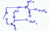
When switch closed on your circuit, we should see 5Volts (minus the saturation voltage of emitter to collector of PNP transistor) on Output 2 and 0Volts (plus the collector to emitter saturation voltage of the NPN transistor) on Output 1
.....UNLESS we have the influence of JoeWawaw's 5Volts via 100ohm resistor on top side of switch
Then when switch is then opened we should see 0Volts on Output 2 due to resistor on PNP collector tying Output 2 low while PNP transistor is not biased on and 5Volts on Output 1 due to resistor on collector of NPN transistor tying Output 1 high while NPN transistor is not biased on.
I hope we can both agree on this?

The following quote is what JowWawaw was asking for. The circuit I provided gives a a near 0-5V swing on one output and a near 5-0V swing on the other; the change occurs when the switch is pressed.
Yes, that was at the beginning of his post that I read that......then it changed from being a single switch, to a matrix keypad, ......then again to ......
Quote ""So I'm trying to "demultiplex" an array of 12 switches arranged in a 3x4 manner, one of those keypad digits thing.
It comes with 12 switches multiplexed to 7 pins, 3 for one side, 4 for the other, i want to rearrange it so that a i have all 12 pins available.
My idea was to have this circuit connected twelve times from each "anode" to each "cathode", then when one switch is pressed, the voltage alternates only on those two pins that connect that switch, which would then be connected to some gate that would give me an output. " Unquote

Dougy83, on your circuit you have 2 outputs per switch, not one.
With reference to above paragraph red text, Does this not mean that JoeWawaw wants one switch to vary one output?
.....again, I'm not arguing, .....just discussing and stating where topic confusion lies
 
I didn't read all of your passive aggressive post, but I drew some pictures for you. These include a 100R pull-up and pull-down on the switch that you mentioned. Circuit functions in the same manner with or without them.
 

Attachments

  • ScanImage5.png
    ScanImage5.png
    57.9 KB · Views: 123
I didn't read all of your passive aggressive post.

Flip sake Dougy83, that's a bit rough!

Is there an unhidden rule that no-one is allowed to discuss or question your reply to posts?

If not then may I (request?) to continue......

Yes, I agree, your circuit will theoretically work, but for how long practically?

Most cheapy keypads I've seen online are contact current rated around approx 20mA

Your base current on NPN (lower transistor ...when switch is closed)...... is 43mA

where I = V/R .....
0.043A = 5V{supply} - 0.7V{NPN Base Emitter Voltage} ....divided by 100 {100ohm resistor}

....that equates to your 12 switch keypad drawing a massive 0.516 amps if all 12 switches were to be pressed simultaneously .....which, yes I know, isn't an issue here.

Unless you place an additional current reducing resistor on its base, or implement a "digital transistor" here, for example a DTC114ECA. .... 43mA is also a bit on the harsh side of things for such a multiplex keypad digital circuit design.
.....
 
Try using a Thevenin equivalent when calculating the base current; you'll get a better answer.

And no, I don't think my statement was rough; especially when you follow up with some unctuous rhetoric.
 
Try using a Thevenin equivalent when calculating the base current; you'll get a better answer.
Irrelevant......for such a simple circuit....you'll find my current estimation close enough to prove you are over-biasing the NPN transistor.


And no, I don't think my statement was rough; especially when you follow up with some unctuous rhetoric.
Thanks, cheers Dougy83, I can only take that as quite a compliment from your Google dictionary index of personal criticisms.

But lets get back to the point.....since you seem to be putting more efforts into answering with another question and getting personal rather than amicably discussing your circuits inadequacies

Try at least to add less confusion for other forum users and redraw your circuits outputs in a similar named format. (see attach)
 

Attachments

  • switch complementary outputs.png
    switch complementary outputs.png
    12.4 KB · Views: 120
  • ScanImage5.png
    ScanImage5.png
    57.9 KB · Views: 145
I haven't yet seen an answer to whether my circuit with the Zener diode would work... when it is off, the top output would be high, and the bottom low, when the switch is pressed, theres a voltage divider formed, the Zener diode will not conduct at 2.5V, and the bottom's voltage would be sufficiently strong enough to activate another gate. I'm probably going to use a higher resistor value for the two connected to 5V and ground to not waste too much current
 
I haven't yet seen an answer to whether my circuit with the Zener diode would work... when it is off, the top output would be high, and the bottom low, when the switch is pressed, theres a voltage divider formed, the Zener diode will not conduct at 2.5V, and the bottom's voltage would be sufficiently strong enough to activate another gate. I'm probably going to use a higher resistor value for the two connected to 5V and ground to not waste too much current

Hi JoeWawaw,
I can see what way you are thinking here, but I also see two problems that you may have overlooked within your circuit.

First of all, your 4 volt zener (as would most zeners) require approximately 10 to 20mA flowing through it to conduct and perform as designed within it's voltage range. Unfortunately I do not see any path through which this 10 to 20mA can flow in your circuit. Perhaps you may think that it could flow through the input of your inverter chip, but no, the input to logic inverters are high impedance and only require micro-amps on inputs to switch output states.
It cannot flow through your 1Mohm resistor to ground, as this also is too high of resistance to allow 10 to 20mA to flow, allowing your zener to perform as designed.

Secondly, when your switch is closed, yes, you are right to say you have created a potential divider circuit with the two 100ohm resistors, which as you say will produce approx 2.5V at midpoint between the resistors, but you have to look at why 2.5V is a big no-no in some logic circuits....you are in what designers call "the grey no-go area" for logic gate inputs especially if you intend using CMOS logic gates.
For a great detailed explanation on this, have a peep at
Code:
http://www.allaboutcircuits.com/vol_4/chpt_3/10.html

so my thoughts on your circuit is that it probably wont work the way you expect it to.

hope this helps,
Rotarymaker
 
JoeWawaw, you could fashion something similar to what you've proposed and it could be made to work. You'd probably want to use TTL compatible input (e.g. 74HCT') buffers as they have inputs specified to operate with a lower threshold.

OTOH, you'd get a more reliable function using something based on the first circuit I posted feeding into the decoder circuitry. Alternately you could further simplify that circuit, removing the NPN (thus simplifying the decoder also by removing the inverter) to something like the attached circuit. For a 3x4 keypad matrix, you'd only need 3 transistors and 6 resistors on the rows, and 4 resistors on the columns. The decoder then consists of just a single AND gate per switch.
 

Attachments

  • matrix decoder.png
    matrix decoder.png
    13.5 KB · Views: 120
Status
Not open for further replies.

Latest threads

New Articles From Microcontroller Tips

Back
Top