jamesportman
New Member
Hi,
Hope it's OK to ask for help as my first post, I just found this forum,
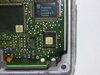
I am looking for more information or replacement for an IC I have here, attached a picture, I am referring to the top right IC.
The chip sits between a CPU which has 16 address/data lines, and a parallel ROM chip which has 16 address lines and 8 data lines out,
so it is doing some buffering between the two due to the limited number of bus lines on the CPU side.
It accepts a 16-bit/line address, holds that and passes it on to a ROM chip address lines, then accept 8 bits back from the ROM chip (while still holding the address (probably)), then passes the 8 bits back to the CPU. (When passing data back to the CPU it probably sends the 8 bit data back on lines 0-7 then leaves the rest as 0 I assume)
The CPU has a pin to mark "address valid", which I expect triggers the above to happen, I think it also has a pin for "external access" which would basically turn on the buffer and ROM chip (think chip enable pin).
The chip is marked with some info that is apparently not a part number, including:
PCC3530HP, 305272, DSD5449 A Y, TAIWAN.
The board in this case is from a Rover (English car) ECU, from around 1995.
The CPU in this case is the Intel AN87C196KD
The ROM is AT27C256 (AT27C256R?)
Summary:
Can anyone could even give me more information on what type of chip this is, or what it's called?
Edit: The closest thing I've seen so far is a tri-state buffer
Alternative: There are large pads for the CPU address/data lines so I could solder to those and use a completely different buffer and ROM chip as an option, but I need to figure out exactly what the buffer chip is, and to make something that acts in the same way/same timing.
Thanks for any help
Hope it's OK to ask for help as my first post, I just found this forum,
I am looking for more information or replacement for an IC I have here, attached a picture, I am referring to the top right IC.
The chip sits between a CPU which has 16 address/data lines, and a parallel ROM chip which has 16 address lines and 8 data lines out,
so it is doing some buffering between the two due to the limited number of bus lines on the CPU side.
It accepts a 16-bit/line address, holds that and passes it on to a ROM chip address lines, then accept 8 bits back from the ROM chip (while still holding the address (probably)), then passes the 8 bits back to the CPU. (When passing data back to the CPU it probably sends the 8 bit data back on lines 0-7 then leaves the rest as 0 I assume)
The CPU has a pin to mark "address valid", which I expect triggers the above to happen, I think it also has a pin for "external access" which would basically turn on the buffer and ROM chip (think chip enable pin).
The chip is marked with some info that is apparently not a part number, including:
PCC3530HP, 305272, DSD5449 A Y, TAIWAN.
The board in this case is from a Rover (English car) ECU, from around 1995.
The CPU in this case is the Intel AN87C196KD
The ROM is AT27C256 (AT27C256R?)
Summary:
Can anyone could even give me more information on what type of chip this is, or what it's called?
Edit: The closest thing I've seen so far is a tri-state buffer
Alternative: There are large pads for the CPU address/data lines so I could solder to those and use a completely different buffer and ROM chip as an option, but I need to figure out exactly what the buffer chip is, and to make something that acts in the same way/same timing.
Thanks for any help
Attachments
Last edited:
