Continue to Site

Welcome to our site!

Electro Tech is an online community (with over 170,000 members) who enjoy talking about and building electronic circuits, projects and gadgets. To participate you need to register. Registration is free. Click here to register now.

  • Welcome to our site! Electro Tech is an online community (with over 170,000 members) who enjoy talking about and building electronic circuits, projects and gadgets. To participate you need to register. Registration is free. Click here to register now.

Need help with sawtooth vertical scan on homemade video camera

Status
Not open for further replies.

aussiebloke

New Member
G'day all.

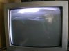
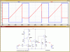
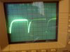
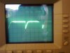
I a vintage video camera enthusiast from Australia and I have built from scratch a 2/3" vidicon tube B&W camera using a 1970s vidicon camera schematic, my camera project can be viewed on my website on this page **broken link removed** . The camera is making pictures however there's a problem with the vertical scan. Basically I am not getting a proper sawtooth waveform for vertical scan and as a result I am getting a vertically squashed picture (see attached image).

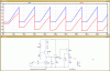
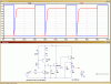
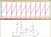
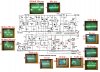
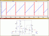
As you'll see in the attached schematic of the vertical section the problem lies between collector of transistor TR19 and gate of transistor TR21. As I understand TR19's base is fed a 1v pulse every say 20ms and during that pulse period TR19 goes to saturation and shorts the current at the collector to ground and then during the pulse off period the 4.7uF capacitor charges up to about 14.5V, and then when the next pulse occurs the process is repeated which is suppose to create a sawtooth waveform. The problem is however the capacitor charges up exponentially giving a non-linear ramp which results in a picture that's vertically squashed at the top but stretches as the vertical scan progresses down the screen. I have experimented with increasing the capacitance which resulted in a better slope that looks more like a sawtooth but the peak voltage drops as capacitance is increased which is the nature of capacitors as they filter out AC ripple, this results in a better picture with more vertical width but more darker due to drop in amplitude.

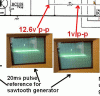
I need to find a way to generate a sawtooth waveform from that 20ms pulse coming from the MC14528 chip with a linear ramp, so I was wondering if anyone here knows of what circuitry I could implement between TR19 and TR21 that would give me a linear charge up ramp to a peak voltage of about 14.5v in a period of 20ms? Any help would be MUCH appreciated.

The schematic for this camera came from a book titled "Amateur Television Handbook" which can be downloaded from here **broken link removed** .
 

Attachments

  • picture.jpg
    picture.jpg
    21.8 KB · Views: 190
  • vertical.jpg
    vertical.jpg
    100.2 KB · Views: 256
hi,
The circuits works as expected using the original transistors and also the later equivalents.

I would say you have a component error most likely the 4.7uF is only a 0.47uF
 

Attachments

  • AAesp01.gif
    AAesp01.gif
    33.8 KB · Views: 164
  • AAesp03.gif
    AAesp03.gif
    35.5 KB · Views: 180
  • AAesp04.gif
    AAesp04.gif
    35.2 KB · Views: 170
Last edited:
G'day. Thanks for the info and diagrams. I'm afraid the value of the capacitor is 4.7uF and I even replaced it with another 4.7uF but it made no difference. I am curious what else would cause the charge up to be exponential like that? Also I noticed the pulse on width you had in the program was 10ms, the actual pulse on width is less than 1ms, I wonder if a very brief on pulse to the base of TR19 could effect the charge up of the capacitor? Probably doesn't but thought I'd ask anyways. And what is that electronic circuit design program you are using, because I want to download it for my use?
 
hi,
I used the notes on your image for the 20ms.??

I will rerun at 1mS, let you know, couple of minutes.!
 

Attachments

  • AAesp06.gif
    AAesp06.gif
    72.1 KB · Views: 159
hi,
Looks fine to me at 1mSec, the pulse only discharges the C1 4.7Cap.

The reason for your non linear ramp is due to the 4.7u charging too quickly, the BC212A is a constant current source, which should give a linear voltage rise on the 4.7u.

Can you scope the actual C1 waveform so that I can see its lower and upper levels

EDIT: measure also at the Source pin of the 2N3819

EDIT2: another source of the problem could be the 5.6V zener, is an ordinary diode.!
 

Attachments

  • AAesp07.gif
    AAesp07.gif
    38.8 KB · Views: 158
Last edited:
G'day. Thanks for the info once again. Attached is the schematic with the waveform readings scoped at various sections of the timebase circuit. I am a little confused with scoping the C1 waveform as putting the scope probe across the capacitor would be the same as putting the probe to the collector of TR19 which I've already done, is that what you wanted me to do? I have the scope readings in larger size and have attached the two significant ones, one at collector of TR19 and the other at the source of TR21. The 5V6 zener diode, what diode shall I put in place of it?

Anyways thank you once again, look forward to any solutions you might have to bring about a proper sawtooth wave for the vertical scan.

hi,
Looks fine to me at 1mSec, the pulse only discharges the C1 4.7Cap.

The reason for your non linear ramp is due to the 4.7u charging too quickly, the BC212A is a constant current source, which should give a linear voltage rise on the 4.7u.

Can you scope the actual C1 waveform so that I can see its lower and upper levels

EDIT: measure also at the Source pin of the 2N3819

EDIT2: another source of the problem could be the 5.6V zener, is an ordinary diode.!
 

Attachments

  • timebase circuit waveforms.jpg
    timebase circuit waveforms.jpg
    284.4 KB · Views: 197
  • TR19 collector.jpg
    TR19 collector.jpg
    26.4 KB · Views: 186
  • TR21 source.jpg
    TR21 source.jpg
    24.5 KB · Views: 154
Most vert deflection systems iv worked on in TV repairs had adjustable feedback in the vert output stage for linearity adjustment.
 
hi,
Had a quick look at your scope images, will look closer later.

About the 5.6V zener, I meant make sure its not a standard diode by mistake, that would also give that problem.

The problem is in that constant current charger circuit.

EDIT: Looking at image #11, you should not be able to get 14.5V pk.??

EDIT2: You could also have TR20 pins crossed over, check the pin out diagram
 
Last edited:
I've just run a simulation as per Eric's circuit with a couple of mods.
(1) If D1 = 4V7 and R2+R3 = 1k4 then a linear ramp voltage on C1 can be obtained (albeit with a maximum of 11V). [N.b. D1=4.7V because I couldn't find a 5.6V zener model in LTSpice!].
(2) If D1 = 4V7 and R2+R3 = 1k4 and C1 = 2uF and a 1k resistor is connected across C1 then the voltage trace for C1 looks very similar in shape to the exponential scope traces posted. This suggests that C1, even if it has been replaced and is nominally 4.7uF, in fact has a lower-than-marked capacitance and is leaky.

BTW, I don't see how a linear ramp from 0 to 14.5V can possibly be obtained with the circuit shown.
If D1 is a 5.6V zener then the emitter voltage of Q2 is ~ 15-5.6+0.6 = 10V. So the maximum C1 voltage of a linear ramp will be when Q2 saturates, i.e. ~ 10V. Beyond that, the C1 charge will be non-linear.
 
alec,
The original circuits works fine, I am convinced that he has a component problem.

For the zeners... back up your standard.dio replace the original standard.dio with the attached standard.txt , change the .txt to .dio first.!
 

Attachments

  • AAesp10.gif
    AAesp10.gif
    36.1 KB · Views: 178
  • Draft6a.asc
    2.5 KB · Views: 118
  • standard.txt
    12.1 KB · Views: 335
If he's not getting a linear ramp, then his constant current source isn't working, either it's wired wrong (most likely), or a faulty component.

It's a simple enough circuit, with nothing to go wrong really.

Check the voltage on the base of TR20 (bottom of the zener), I would imagine it will be low, as the zener is the wrong voltage.
 
Last edited:
........... And what is that electronic circuit design program you are using, because I want to download it for my use?
Eric mentioned LTspice, if you didn't catch that. It's a free circuit simulator from Linear Technology that many of us use for circuit simulation. You just enter the schematic of the circuit and then hit the simulate button. The tutorial will tell you how to get started.
 
G'day all. Going by what's been said, I have checked the voltage drop across the diode and it appeared to be about 2.4v DC, so I replaced the diode, couldn't find a 5.6v zener so I put a BZX79C 5.1v zener in instead for testing purposes. Then checking the voltage drop again, no different, I am getting only 2.4v drop once again. I then disconnected R2, R3 and Q2 (TR20) and tested the voltage drop and the zener was working properly giving it's specified voltage drop of about 5.1v. Having R2, R3 and TR20 in parallel seems to lower the voltage drop for some weird reason. I also checked TR20 which I'm using a BC558 (equivalent to BC212) and it's working fine, even pulled it out and tested it! I am now totally whipped!
 
hi.
In simulation measuring across the 5.6V zener, I read 5.5V, which is within specification.
Across R5 [5k6] should be ~9.5V

Measuring across R2, R3 [ set at 1K each] I get 4.7V, which is what I would expect.

The current thru R2, R3 is averaging 2.3mA

Try this, remove the 2N3819 FET, check the waveform across the 4.7uF

EDIT:
Can you post a clear image of the PCB showing the area of the 4.7u and the transistors.??
 
Last edited:
I'm sure I posted something yesterday but it seems to have gone AWOL.
Eric, thanks for the updated component file, now installed.
 
G'day all. I finally found the exact problem, it was the FET transistor TR21 causing the capacitor to charge too quickly, as 2N3819s are not available at my local Jaycar Electronics store, I used a close equivalent suggested by a tech friend of mine which is a MPF102. I wonder if the slight differences of the MPF102 would be the main cause of this issue or would it be something else as I did have the transistor in the right way plus there's no shorting across any of the pins? Anyhow testing the waveform at the 4.7uF cap with TR21 removed I got a perfect sawtooth waveform at a much lower voltage though forgotten what the voltage was. Anyways just have to get around this transistor issue and all should be good! :)
 
hi,
Pleased to hear you are making progress.

In simulation, the MPF fet performs as well as the 2N3819.?

I wonder if your MPF is defective or a different pin out.?
 

Attachments

  • AAesp02.gif
    AAesp02.gif
    36.8 KB · Views: 149
Problem solved!!! :D It turns out the MPF102 transistor was defective, just bought a few more from my local electronics store and have replaced it and BINGO, perfect sawtooth waveform and full screen picture!!!!! :D Will post pictures soon, also have made a video from the video out of the camera which will go to YouTube soon too. The vidicon tube seems to has very poor sensitivity in low light so the best pictures I could make were from pointing it to my computer screen. Anyways I am now a very happy man!!! :)
 
Problem solved!!! :D It turns out the MPF102 transistor was defective, just bought a few more from my local electronics store and have replaced it and BINGO, perfect sawtooth waveform and full screen picture!!!!! :D Will post pictures soon, also have made a video from the video out of the camera which will go to YouTube soon too. The vidicon tube seems to has very poor sensitivity in low light so the best pictures I could make were from pointing it to my computer screen. Anyways I am now a very happy man!!! :)

hi,
Looking forward to seeing your pics.

Whats the vintage of the Vidicon tube.? [new or old]
 
Status
Not open for further replies.

Latest threads

New Articles From Microcontroller Tips

Back
Top