Electro Tech is an online community (with over 170,000 members) who enjoy talking about and building electronic circuits, projects and gadgets. To participate you need to register. Registration is free. Click here to register now.
Welcome to our site! Electro Tech is an online community (with over 170,000 members) who enjoy talking about and building electronic circuits, projects and gadgets. To participate you need to register. Registration is free. Click here to register now.
ZipZapOuch I guess you are unable to admit you're wrong even in light of overwhelming evidence. *Shrug* Perhaps you should stop picking fights.
If MrDEB follows your advice, will you take responsibility if the MOSFETs he uses next time don't exhibit the same rare property of an isolated tab? If indeed the current ones do (hint, they won't)?
I'm confused about your last paragraph. Are you saying I'm not responsible for damage to Mosfets on the current project but I will be responsible for damages on his next project that uses Mosfets? Or do you mean something else? And, are we assuming he tests the continuity as I advised or that he doesn't remember to test continuity? And, will I be responsible for ANY damaged Mosfets no matter how they are damaged or only if he has the unique requirement of mounting multiple Mosfet thermal tabs to the same heat sink? Please advise, then I'll answer your question about taking responsibility for MrDeb's actions.
MrDEB Sorry for the extraneous distractions. Post #25 may have been lost in the noise. Would you answer those questions? It does not seem like heating should be a problem with your MOSFETs, so we must be missing some key details.
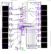
I want to AVOID ANY HEAT. HERE IS MY PRELIMINARY BOARD .
This has to be the most difficult board I have done. Had net connection issues.
I need to add/change labels.
Many '44Z' documents oddly omit the answer to this basic question. ( Gap between EE & ME documentation)
The base p/n is obsolete yet on hand yet was produced by many being off patent. New p/n suffixes exist.
TO-220 variants are generally electrically "hot tabs" to the "normal" output pin unless specified "isolated tab"
The thermal resistance is generally proportional to the electrical capacitance and insulation voltage rating due to the insulator thickness, as well as ; dielectric constant, contaminants, tension, conductive particulate content and other factors.
There are minor differences between TO-220-3 and TO-220-AB off-topic
Using est. 1 sq.in. 1 sided 1oz Cu might better than double the total radiation area of the device and reduce Rja from 62 °C/W to less than 30°C/W depending on the above variables.
Even 1 watt is "no sweat" at this rise above ambient if nothing else is overlooked such as the enclosure Rth or inaccurate Pd estimate or unspecified "do not exceed case temp = TBD "
Don't sweat the small stuff when one piece of important info seems to be missing on most datasheets.
IMHO, Vishay brand normally produces off-patent devices (> 10y or more) and acquires technology from the OEM with a wide technology base. They also produce the IRLZ44 but do have a bunch of fabrication patents.
January 13, 2015 – Infineon Technologies AG announced the closing of the acquisition of International Rectifier who bear the prefix of all p/n starting with IR
I want to AVOID ANY HEAT. HERE IS MY PRELIMINARY BOARD .
This has to be the most difficult board I have done. Had net connection issues.
I need to add/change labels.
eTech is right. All of your power connections should be BIG FAT traces. How are you expecting those thin traces to supply 2+ amps? They certainly won't AVOID ANY HEAT....well, after they pop like fuses they will!
The MOSFETs on the left have a break in the tiny ground connection, and one of the gates has no connection. The MOSFETs on the right appear to be missing ANY ground connection.
You don't have mounting holes for THE MOSFETs.
You can still use a ground plane on the bottom layer, separate from the heat sink areas.
Presumably, you have copper areas top and bottom? They need vias stitching them together.
will look at the suggested corrections. The CHECK NET CONNECTIONS says everything is good but will verify.
As for the trace width, I need to poor over and increase suggested traces.
Have yet to add the bottom heat sinks.
As for the generation of heat etc. the enclosure is basically a sealed enclosure and the 12v 5W transformer is in same enclosure. Looking at attaching an aluminium grate to top of enclosure for cooling issues?
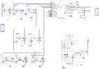
Checking the net list only verifies the board connections match the schematic, not that the connections are proper. Take time to perfect the schematic before laying out a board.
For example, these ground connections appear not to be made. You have a number a number of identical blocks. Draw one. Make it neat and clean, no jaggy lines or lines across components, and verify every connection. Then duplicate it however many times you need to.
For example, these ground connections appear not to be made. You have a number a number of identical blocks. Draw one. Make it neat and clean, no jaggy lines or lines across components, and verify every connection. Then duplicate it however many times you need to.
You are almost certainly wrong, the connections look sound - just very poorly drawn. The line from ground goes UP, LEFT, and then DOWN to connect to the connection 'dot' at the bottom of the resistor. If it wasn't making proper contact, the line would vanish leaving it obviously not connected.
What he needs to do is pull the Gnd symbols down a bit, and then drag the horizontal line down until it's in-line with the source of the FET's. Same with the other badly drawn connections.
Ground connections are missing on the circuit board, yet the net list matches. So you explain how that happens.
But I greatly appreciate your feedback, even though you missed the point of starting with a clear, concise, verified and double-checked schematic before laying out a board.
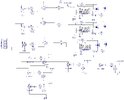
The PC board should only show a reference designator (and maybe an outline) for each component. There are exceptions, but very rare. If you place values, and then, if a value needs to be changed, the PCB has to be modified is some way. This is bad, and sometimes costly. Part values (as well as reference designators) should be shown on schematics.
All of the lines shown in pick should be ground lines. This isn't every ground line but it does include significant traces to the MOSFETs that may be handing 2 amps or more each. I defy you to find any trace between some of these segments, and there are no traces on the board that will handle 2 amps or more. If the board agrees with the netlist, the netlist is deficient. If the schematic is incorrect, the board built in accordance with its netlist will be incorrect. A clear, neat uncluttered schematic is the first step.
Additionally, there's a resistor pad marked in orange without a connection.
I'm not trying to be argumentative; I'm trying to explain problems and ways to build a better circuit board. Not that it will be heeded.
If a ground plane was used, that eliminates (potentially) the ground issue. But the +12v traces still need to carry large currents, These "fuseable link" traces certainly aren't up to the task.
will look at the suggested corrections. The CHECK NET CONNECTIONS says everything is good but will verify.
As for the trace width, I need to poor over and increase suggested traces.
Have yet to add the bottom heat sinks.
As for the generation of heat etc. the enclosure is basically a sealed enclosure and the 12v 5W transformer is in same enclosure. Looking at attaching an aluminium grate to top of enclosure for cooling issues?
With an enclosure, there is no convection air flow so those thermal resistances values I quoted will likely double and that was before you added another heat source, the transformer instead of a power jack and external DC. It's not a lot of power, but it's not a good way to reduce temperature rise. It could be vented a metal enclosure.
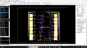
ALMOST DONE increased the ground traces to 1mm. Plan to use 2oz copper
a little trace squiggle needs to be straightened out.
The ground is connected to the top and bottom pours.
According to online calculators on trace width, I used 3A for overkill.
Remember, the current from ALL of the MOSFETs goes through those ground connections. Why not make those ground traces FAT? There aren't other traces in that area.
Here's a thought question for you. Where does all the current the MOSFETs switch come from? I believe the 12 volt in connection is at the bottom end of the board. Many of the strips connect at the top of the board. Do you think that thin wandering 12 v trace from the bottom of the board to the top is up to the task?
How are you holding the MOSFETs against the board? Those holes I mentioned before are kind of important.
This site uses cookies to help personalise content, tailor your experience and to keep you logged in if you register.
By continuing to use this site, you are consenting to our use of cookies.

.png")