Electro Tech is an online community (with over 170,000 members) who enjoy talking about and building electronic circuits, projects and gadgets. To participate you need to register. Registration is free. Click here to register now.
Welcome to our site! Electro Tech is an online community (with over 170,000 members) who enjoy talking about and building electronic circuits, projects and gadgets. To participate you need to register. Registration is free. Click here to register now.
I will get a screenshot of the top and bottom today.
As for the mounting holes, the data-sheet is a little confusing, so I plan to bend over a MOSFET pin, then mark on a piece of paper the exact mounting hole location.
Looks like there is a fair amount of room around the mosfets. I don't think 2oz copper is needed. You can probably just fatten traces and add pours to satisfy the mosfet load current requirements and stay with standard 1oz copper (saves a little $).
Be aware that if the PCB is 2oz copper, it'll take more heat to solder components.
You've ignored thr comments about stitching the top and bottom layers of the heatsink zones together. If you don't understand something, ask instead of ignoring it.
"Reduce Heat dissipation
"When current flows through a conductor, such as a trace or via, a certain amount of heat is generated due to the resistance of the material. In high-current applications, this heat generation can be substantial. By strategically placing stitching vias, designers can create a pathway for heat to flow from areas of high heat generation to areas where it can be dissipated more efficiently. This helps in spreading out the heat, preventing localized hotspots, and maintaining more uniform temperatures across the PCB."
Put small diameter vias around the edges of each heatsink area to allow for heat transfer through the board. The vias must be connected to the same net as the MOSFET tab in each area.
I haven't got to adding the itching yet, as well as the mounting holes.
Been contemplating moving the MOSFETs closer together as suggested. Making the board narrower.
Been assembling a 555 prototype board, but it fails to work. Thinking a bad chip from Tayda?
Tayda has been reliable in everything I've ever bought there. Faulty chip wouldn't be the top of the list suspect.
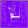
I ask again: where are the 12v connections to the strips? Is it from the pin headers? No traces that I can see that connect to 12v are capable of carrying multiple amps.
If I was doing this - creating many duplicate heatsink areas - I'd create a footprint once, then duplicate it as necessary. Do ALL the work once to get it perfect, then duplicate it.
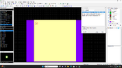
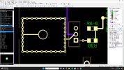
Start with creating a horizontal TO-220 footprint as shown here.
Then add the desired heat sink areas with stitching vias.
Then plop them in the desired positions on the board. Notice the soldermask-free areas under the TO-220 packages. Much simpler to lay it out once and add all the details first.
Yeah, I know this is an effort in futility, but I tried.
Where are the 12 volt traces? The 2+ amps you're switch for each strip have to come from somewhere. Looks like power comes in at the commector at the bottom of the board and goes out to some of the strips at the top without any substantial trace providing that power.
12v+ goes directly to the LED strips and the MOSFETs ground the strips.
I just created the heat sink area, then copied and pasted it into the position.
The 12v + on the pcboard are for powering the 12v+ on the strips.
Yes. I understand that. But as far as I can see, none of the traces on the board will carry the many amps of current drawen by the LED strips. If each MOSFET is switching 2+ amps, how is that current getting to the strips?
12v+ goes directly to the LED strips and the MOSFETs ground the strips.
I just created the heat sink area, then copied and pasted it into the position.
The 12v + on the pcboard are for powering the 12v+ on the strips.
Just something to be aware of:
Most integrated Schematic Capture/PCB layout tools provides an automated feature that keeps the schematic "synchronized" with the PCB (or visa versa) when changes are made. It usually requires manual initiation. This avoids missing components or wiring errors between the two. Its a good idea to "synchronize" the changes whenever they are made to ensure the schematic matches the PCB and avoid costly mistakes.
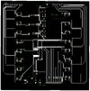
attempting to stitch the top pad with the bottom pad but ?
Keep getting errors as pictured in attachment.
Tried different heatsink pads (courtyard, signal etc. Tis is using a smd pad with one via
Put small diameter vias around the edges of each heatsink area to allow for heat transfer through the board. The vias must be connected to the same net as the MOSFET tab in each area.
Please realize, the net for each MOSFET will be different if you're "adding this on" rather than defining a footprint as I explained above. The net will be the drain of the associated MOSFET.
This site uses cookies to help personalise content, tailor your experience and to keep you logged in if you register.
By continuing to use this site, you are consenting to our use of cookies.