Continue to Site

Welcome to our site!

Electro Tech is an online community (with over 170,000 members) who enjoy talking about and building electronic circuits, projects and gadgets. To participate you need to register. Registration is free. Click here to register now.

  • Welcome to our site! Electro Tech is an online community (with over 170,000 members) who enjoy talking about and building electronic circuits, projects and gadgets. To participate you need to register. Registration is free. Click here to register now.

Making a Bluetooth adapter for a Car Phone from the 90's

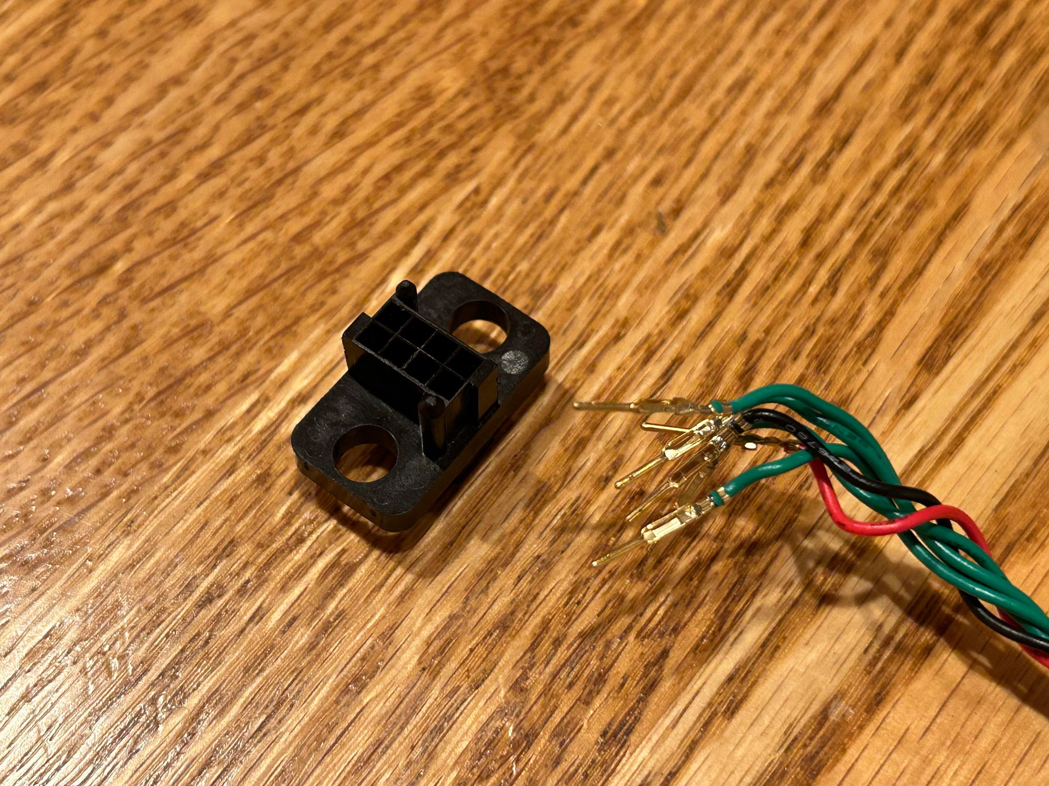
Well, that was easy. Some 22-gauge solid core wire worked great as a de-pinning tool this connector.
1706924306612.png


I like that this is a simple, non-destructive, and easily/reliably reversible "borrowing" of an original part.

Next I have to see how easily I can de-solder the female pin header from the transceiver circuit board. Good thing I have 7 spare phones, and one of them already doesn't work reliably.
 
I assembled the breakout boards for the load switches. It was actually very easy to solder these.

1706988160450.png


Much smaller than the relays they are replacing :)

1706988195149.png


And MUCH more efficient too!

When the car phone was powered on and idle (handset "on-hook", backlight off, etc., but with an active Bluetooth connection to a cell phone), my circuit was previously drawing ~61 mA with the relays and the transistor used to switch the relays. Now with the load switches, it only draws ~49 mA! No transistor needed because these load switches are directly compatible with MCU digital outputs.

In fact, for a minimal setup, these load switches require nothing more than a decoupling capacitor on their voltage input (1 uF). It's as simple as Vin, Ground, digital enable input directly connected to a MCU digital output pin, and Vout.

1706941623810.png


And right after I took that last picture, the slightly diagonal red wire (the horizontal one in the picture) bothered me, so I went to straighten it by swapping positions between the end of that wire and the battery module power connector wire (vertical red wire on the left side of the picture). Stupid me left the battery module connected while moving things around, and I accidentally reconnected that battery module power connector wire one hole over on the OUTPUT pin of the 5V regulator, feeding 12V directly into the MCU and killing it :facepalm:

Time to place yet another order for a few dollars worth of parts, paying 3 times that amount on shipping, and waiting a week to get the new MCU :banghead:. I may as well order a few of them.
 
Last edited:
I successfully desoldered the socket from the original car phone transceiver PCB:

1706988380523.png


It was actually very easy, using the technique I learned from this video:


It was so easy that I think I'm abandoning my plans to use different connectors with custom risers and mounting plates, etc.

A total of 3 parts have been scavenged from the original phone to be reused with my Bluetooth adapter:

1706988473680.png


The 8-pin connector and header will of course be used to connect the Bluetooth module daughterboard to the main board. The coax antenna connector won't be used in my circuit, but the physical connector itself still needs to be reused so the original antenna can be mounted for a 100% original appearance.
 
Last edited:
Time to place yet another order for a few dollars worth of parts, paying 3 times that amount on shipping, and waiting a week to get the new MCU :banghead:. I may as well order a few of them.

I mostly order from RS or Farnell at work, and as long as you meet the minimum order charge (about £30 as we have accounts at both) then it's free postage, and delivery is next day. There's always something you can bung on an order to take it over £30 :D - for example, we use a lot of potting resin, and a 1kg bag of that is getting towards £30 now.

For Chinese orders, where delivery is slow, I never order one of anything - I order multiples, so if I need another (or I kill the one I wanted) I've already got them to hand, and the parts are generally cheap enough anyway.
 
I'm just one person working on one project. No business account. No items/materials that I regularly use in significant quantities to pad out my orders. No free shipping offers from the major suppliers here in the US (although I did find some likely outdated claim that DigiKey will ship for free if you pay via check sent in the mail, but who does that?).

The US is also huge, so even though I am in the US buying from a major US-based supplier, it's still being shipped from ~1200 miles away and takes about 3-5 business days to arrive ($8 USD shipping option). Next day delivery would cost $25 USD. Or I could save money on the "economy" shipping option for $5 USD, but then delivery time is 5-15 days.
 
I figured out a way to mount my Bluetooth module in the "transportable cover" of the car phone: Hide it in the shell of the original battery pack!

Here's the battery pack split in half and emptied out:

IMG_1911.JPG


This is my custom wiring that connects my Bluetooth module to the original electrical connector for the "transportable cover":

IMG_1913.JPG


Bluetooth module in the battery pack shell. I had to notch out the side of the battery pack to allow the wiring to pass through. I'm using some random pieces of foam to "sandwich" the Bluetooth module inside of the battery pack shell. It's not stupid if it works, right? It passed a vigorous shake test without shifting around inside the shell.

IMG_1914.JPG


Here's the battery pack and wiring installed in the "transportable cover". The area that the wiring passes through is where the original battery charging circuit board used to be installed.

IMG_1917.JPG


And the final fully assembled result:

IMG_1918.JPG


It looks completely original :). And it didn't require any non-reversible modifications to anything aside from the battery pack
 
I decided to take a look at inrush current and play around with the inrush current limiting feature of the load switches I'm using. I'm focusing on the 12V switched power supply to the handset because this is something that I can measure with both the original car phone and with my circuit for comparison.

I used a 1 Ohm resistor in series with the power supply to the handset so I could measure voltage drop across that resistor with my oscilloscope and conveniently have a 1:1 conversion of volts to amps.

Here's the inrush current to the handset when powering on the original car phone:

1708312771493.png


X-axis is 500us per division, Y-axis is 200mA per division (same scale for all graphs in this post).

Peak inrush current is 680mA.

And here it is with my circuit using a load switch to turn power on to the handset as instantly as possibly (no inrush current limiting):

1708315158093.png


Much higher peak of 1.2A, and a rougher shape.

I was able to configure the load switch to limit voltage rise such that the peak inrush current is closer to that of the original car phone, but of course that comes with a limited initial voltage rise too (ramps up over about 1ms), which doesn't match the original car phone power-on voltage rise (pretty instant rise initially), and the shape after the peak is still quite different from the original car phone:

1708315205239.png


So I'm not really sure where to go from here. Should I be concerned about figuring out how to smooth this out? Should I even care about trying to limit inrush current to ~680mA like the original car phone? The load switch itself is rated for 2A continuous, so that's not a limiting factor.

If there's really no harm in having the higher 1.2A inrush current, then I could keep my circuit simpler. FWIW, I did also look at the output of my 5V regulator and did not see any substantial voltage dip, so I don't think I'm at risk of any instability or brown-outs of any of my 5V components during power-on.
 
Last edited:
It's taking forever to prepare to order my PCB through JLCPCB. I originally pre-ordered some parts they don't normally stock on Jan 18. On Jan 31, I received an email to inform me that one of the parts (MAX4619 analog switches) is old stock from their supplier with a production date from the year 2012 and asked me if this was OK. It seemed iffy.

I found that there is a slightly different part number for the same exact part, but just packaged differently (reel vs tube, or something like that), and asked if they could check if their supplier has newer stock of that aprt number. They said that I would have to order the part and they would have to process the order to find out. They recommended that I order the part through global sourcing instead.

So I ordered the part from Mouser through global sourcing on Feb 1. Today I received a notification from PayPal that I was receiving a refund from JLCPCB. No email or message from JLCPCB about the cancelation. Only a refund. I emailed support and the response I got was that the order was canceled "due to the order restriction by Mouser", whatever that means. They suggest that I pre-order the part from JLCPCB now... going in circles.

I double-checked Mouser's website, and they have over 2000 of the part in stock, so I don't understand why there was a restriction.

So now I am trying to pre-order the slightly different part number through JLCPCB pre-order and hoping their supplier has more recent production dates of that part.

If not, should I just go with the 12-year old parts? Or try global source from another supplier? Or just give up and order the part myself and deal with soldering it myself?
 
More JLCB frustration/confusion...

In the past two days I have received 2 messages on my account through the JLCB website that are completely blank. I think they may just be status updates about my recent new part order, because its status has now advanced to "Purchasing". I contacted support about the blank messages and verified with them that it is not a browser-specific issue, not a cache/cookies issue (problem exists in multiple different browsers, in private/incognito windows, etc).

They asked me for my login info including password so that they could login as me and look at it.... uhh, hell no! Support should have some superuser abilities to "impersonate" a user to investigate user-account-specific issues. I'm never handing over my password, especially since I use my google account to login to JLCPCB (not just an isolated JLCPBC login).

Then today I get an email about a global sourcing part order cancellation:

We are sincerely sorry to cancel and refund this order as we do not support to assemble this part at present. Sorry for the inconvenience caused.

No indication of what part or order number this email is referring to. Even more confusing is that I did not have any global sourcing part orders! No change in status of any of my pending orders.

So now my concern is that this was a delayed notification of why my analog switches component order from Mouser was cancelled, despite support previously telling me it was an "order restriction" on Mouser's end. Now I get to wait 1-2 weeks to see if my new order for the same part comes through, or if they cancel that one for unclear reasons too.

Another part I was waiting for just arrived in their inventory today, so this problematic analog switches component is the last part holding me back from placing my PCBA order. I'm seriously contemplating just placing my PCBA order without that part, order that part myself from mouser, and deal with soldering those 16 pins myself. If my parts order does not get cancelled, then I've wasted $13 USD on a parts order I did not use (but can use in a future order), but I get my assembled PCBs 1-2 weeks sooner.
 
I solved an annoying problem with a glorious hack...

First, a refresher on my "power off" strategy: It's way simpler and more robust to reboot the MCU to fully reset all memory/state rather than write code to explicitly re-initialize EVERYTHING. So that's how I power off. Reboot the MCU, and MCU enters a "sleep" state by default after some basic initialization. A couple pin input change interrupts can wake the MCU to allow it to decide whether to finish initializing and power everything on, or just go back to sleep if power-on conditions are not met.

This works great for basic power on/off flows because the MCU will stop enabling the load switches for switched power by default when rebooting - they require high signal to power on.

But I have some situations where I need to restart rather than power off. To handle this, I store a value in EEPROM before rebooting, then upon booting I check for that value in EEPROM to decide whether to immediately power on, or go to sleep. But the load switches briefly lose their "enable" signal from the MCU while the MCU reboots, which causes a brief flicker of power interruption to the handset, Bluetooth module, and audio circuitry. This looks/sounds pretty "glitchy" because it causes a flicker on the handset display, backlight turns off for a second until it is turned back on during the startup sequence, and it causes an audio "pop" sometimes.

So my hack is to invert the load switch "enable" signal from the MCU with a transistor so that the load switches are enabled by default unless the MCU explicitly outputs a high signal to disable them. This allows power to remain on while rebooting for a restart. I just had to invert some power on/off logic a bit. Upon booting, I must explicitly disable switched power before entering the sleep state if not powering on immediately.

1708749712657.png


The downsides to this hack are:
  • When initially connecting power to my circuit, the load switches will be immediately enabled (powering on the handset, etc.) for a small fraction of a second before the MCU reaches the point of initialization where it disables switched power. A brief flicker can sometimes be seen on the display.
    • Not really a problem because the circuit should have constant power supply in normal usage. It will only completely lose power if disconnected from external power AND the batteries discharge down to the low voltage cutoff protection level (which is below my own "low battery" threshold where the user will have been warned of low battery, then I automatically power off and refuse to power back on until battery voltage increases above a threshold). This power flicker would occur when connecting external power to charge the batteries after they have been fully discharged.
  • Some power must be wasted to "hold" the switched power "off" via the transistor.
    • I minimized this by using 1M resistors for both the base and collector of the transistor.

I still think it's better than trying to reinitialize without a MCU reboot, which would be a lot of programming effort with a lot of risk of missing something that needs to be reset, which could cause obscure bugs that are hard to diagnose.

BTW - TI does offer a few load switches that are "active low" instead of "active high", which would allow me to get rid of the transistor inverter. However, there are very few "active low" options, and none of them can handle the 12+V I need to switch for the handset.
 
Last edited:
Couldn't you just add a series resistor & parallel cap to "filter" in the on-off signal so brief glitches are ignored? A few tens of mS delay in switching should have no adverse effects?

I'd advise against using a transistor with such a high value load and no base-emitter resistor - if it gets hot (eg. a car left in the summer sun) it may develop enough leakage to switch the load under some conditions.

If it works with such a high impedance drive, you could also just have a pull-up instead of a pull-down on that pin? The MCU output would initially be tristate so it would have no effect until the output is reinitialised.
 
If it works with such a high impedance drive, you could also just have a pull-up instead of a pull-down on that pin? The MCU output would initially be tristate so it would have no effect until the output is reinitialised.

And this is exactly why I post my ideas and solutions here: so someone can point out how over-complicated I made it :)

I'll try configuring that pin as open-drain with an external 1M pull-up resistor, so even after MCU initialization, I'm switching between tri-state/floating (load switches enabled) and low (load switches disabled). This is fewer components than the RC filtering approach you suggested, and keeps things simple with no additional delays that would be introduced by the filtering.
 
I received my partially-assembled PCBs from JLCPCB yesterday, and finished assembling one today. I'm still a bit in shock at how well everything physically fits and aligns. And the circuit itself seems to be working as intended! Sound quality is pretty good. I think it's better than my perf-board prototype (but haven't directly compared yet).

I still need to do a lot more testing to verify everything is working correctly, but it looks good so far.

1710477688138.png


1710477727687.png


1710477758220.png
 
Here's some side-by-side comparisons of an original car phone and one with my new Bluetooth adapter installed.

The main circuit board in the transceiver
Left: original
Right: modified

1710552483862.png


Transceiver with the lid installed
Left: original
Right: modified

1710552510542.png


Connections for external power supply, handset cord, and external microphone (for speakerphone)
Top: modified
Bottom: original

1710552531038.png


Inside the "transportable cover"
Left: original (battery charging circuit)
Right: modified (Bluetooth module)

1710552546117.png


My Bluetooth module hidden inside of the emptied out shell of an original battery pack
Left: original
Right: modified

1710552557783.png


Transportable cover fully assembled
Left: original
Right: modified

1710552583218.png
 
I made a video demonstrating that the new Bluetooth adapter design works, followed by disassembly to see how everything fits inside:


And here's some disassembly photos:

1710773661029.png


1710773729437.png


1710773767076.png


1710773812022.png
 
One of my extremely rare "Hands-Free Controller Unit" modules quit working today while I was testing it with my new PCB circuit :(. All the audio through the module quite working (both audio output and microphone input pass-through to the car phone transceiver).

This is the module that was severely water damaged and non-functional before I cleaned it up, replaced all the capacitors, and bypassed a few damaged traces. But this is also the first time I tested this module together with my audio circuitry using a pair of INA105's to generate the differential audio output instead of the DRV134. So I'm not sure whether this was a random failure due to the previous water damage, or if my circuit somehow triggered a failure.

Looking at the datasheets, the INA105 has a much lower output impedance (0.01 ohm vs 50 ohm), much lower output capacitive load (1 nF vs 1uF), and higher max output current (+/-85 mA vs +40/-10 ma). I don't really understand the consequences of the differences in output specs. Is it possible that this could have caused damage to the audio circuitry that receives this output as input? (I have no idea what the input specs/requirements/limits of the "Hands-Free Controller Unit" are).

Here's specs for the INA105 (full datasheet):

1710900218179.png


And for the DRV134 (full datasheet):

1710900331276.png


One small piece of evidence causing me to believe this is a random unrelated failure vs damage caused by my circuit: It did start randomly working again for a while, then quit working again a few seconds later in the middle of a test call. So this seems more likely to be an intermittent bad connection somewhere (caused by water damage corrosion) rather than an out-of-spec output from my circuit permanently damaging an IC in the "Hands-Free Controller Unit".

But I only have one more of these "Hands-Free Controller Unit" modules and will likely never find another again, so I'm super paranoid about connecting my one remaining module to my new circuit and risking damage.
 
The lower capacitive load rating means the IC may oscillate if directly connected to too high a capacitive load.

As long as the output has a series resistor before it connects to the external cable, it should be OK.
 
rjenkinsgb I do not currently have a series resistor. The outputs from the pair of INA105's go directly to the RJ45 connector for the handset cord. Would a 50 ohm resistor be reasonable? That would increase the overall output impedance to just over 50 ohms, similar to the DRV134, right?

Also, if there was oscillation, is this something I would have likely noticed as distortion in the audio before failure (audio sounded fine until it suddenly quit working)? Or would it more likely only be visible on an oscilloscope?

And am I correct in assuming that the risk of this oscillation would be that the voltage could swing outside of the absolute max ratings for the input of an IC in the module?

I just remembered that there is a "speakerphone" IC in that module that both the mic audio and the speaker audio pass through (it manages reducing feedback of speaker audio back into the microphone), so that is a suspect for failure since both speaker and mic audio quit working at the same time. I'll look up the data sheet for that IC to look for info about the speaker audio signal limits.

And finally, potentially related, I just noticed while looking at the original car phone's circuit board that many of the RJ45 handset cord connector pins have a bypass capacitor to ground, including the audio pins and the digital UART pins. What is the purpose of a bypass capacitor for a signal right near a connector? The speaker audio pins have about 0.28 uF caps according to my multimeter. I couldn't get a reliable reading on the others, but they seemed to be down in the nF range.
 
The amps could oscillate, possibly at ultrasonic frequencies; or just distort badly, I'm not sure really.
50 Ohms should be OK.

The caps will be for RF bypassing, to limit the amount of leakage from the transmitter that gets back in to other places via the external wiring.

100pF to 1nF should be adequate for most things, I'd expect.
 

Latest threads

New Articles From Microcontroller Tips

Back
Top