Continue to Site

Welcome to our site!

Electro Tech is an online community (with over 170,000 members) who enjoy talking about and building electronic circuits, projects and gadgets. To participate you need to register. Registration is free. Click here to register now.

  • Welcome to our site! Electro Tech is an online community (with over 170,000 members) who enjoy talking about and building electronic circuits, projects and gadgets. To participate you need to register. Registration is free. Click here to register now.

Why is Common Mode Voltage so Commonly Misunderstood?

Status
Not open for further replies.

vne147

Member
I’m hoping someone can help me answer a question I have regarding the INA196 current shunt monitor.

The INA196 has a common mode voltage range of -16V to 80V. But in the datasheet linked above under absolute maximum ratings on page 4, the maximum voltage you can apply to either the V+ or V- analog input is 18V. I’m sure my confusion stems from a poor understanding regarding the exact definition of common mode voltage, but how could I ever reach a common mode voltage of 80V if the maximum I can apply to an input is 18V?

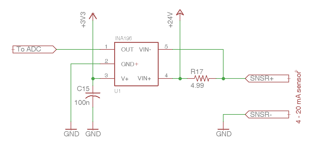
Basically, I want to know if I can use the INA196 as shown in the figure below. Thanks in advance for any clarification you can provide.


cmv-png.101187
 

Attachments

  • CMV.png
    CMV.png
    14.5 KB · Views: 680
The INA196 has a common mode voltage range of -16V to 80V. But in the datasheet linked above under absolute maximum ratings on page 4, the maximum voltage you can apply to either the V+ or V- analog input is 18V. I’m sure my confusion stems from a poor understanding regarding the exact definition of common mode voltage, but how could I ever reach a common mode voltage of 80V if the maximum I can apply to an input is 18V?
In the block diagram on page 1 of the data sheet, note that the first thing in the door for the inverting and non-inverting inputs is a resistor, not a transistor. The resistor is in series with other internal components and basically forms a voltage divider, so that internal voltages do not exceed the power rails.

ak
 
My understanding is consistent with what Ron wrote, and I did see the diagram that AK points out. But, I don't understand how that reconciles with the information in the absolute maximum ratings section. Is that just a typo, or am I not really understanding what is being described in that table?

I'm asking more now not so I know whether or not I can use the arrangement in the schematic of the original post, but more so I know whether or not I have a misunderstanding that needs to be corrected.

Thanks.
 
It's probably an error in the datasheet. I suggest contacting TI technical support to clear up the confusion. And so that they know that something needs to be fixed.
 
It is pin3 that can not go above 18V.
Pins 4,5 can go to 80V.
Agreed, the common mode high side up to 80V { Vin, Vout} allows high side current sensing of a 72V battery, while Vin is 18V max and Vout is low voltage out to ADC.

High side sensing means the common reference is Vin, Vout For high current.

While differential V+ to ground powers the differential amplifier and scales the current out to Vout depending on R sense,,which is typically a 50mV drop at rated I? Not sure of specs.
 
Last edited:
I see specs are user choice 50 -100 mV drop on R sense. and for low currents, 500mV max.
 
My understanding is consistent with what Ron wrote, and I did see the diagram that AK points out. But, I don't understand how that reconciles with the information in the absolute maximum ratings section. Is that just a typo, or am I not really understanding what is being described in that table?
It is *not* a typo. You are applying a specification for some pins to all pins. Operating voltage is limited to the values indicated because that is what the semiconductor devices within the chip can handle. Separate from that, the chip has a couple of resistors that can handle a higher voltage. The higher voltage spec applies *only* to one operating condition (common mode voltage) of only two pins (the signal inputs), and lower voltage specs apply to all other conditions pins.

Datasheets are their own little universe, and real, consequential typos are extremely rare. When in doubt, check your assumptions. You have to know how to read what is *not* in them , as well as understand what is explicit. This comes with time.

ak
 
Last edited:
I have used several parts in this series.
I use them in a way where the (+) and (-) pins are much higher in voltage than the supply voltage.
You can get these parts with built in ADCs inside.
 
It is *not* a typo. You are applying a specification for some pins to all pins. Operating voltage is limited to the values indicated because that is what the semiconductor devices within the chip can handle. Separate from that, the chip has a couple of resistors that can handle a higher voltage. The higher voltage spec applies *only* to one operating condition (common mode voltage) of only two pins (the signal inputs), and lower voltage specs apply to all other conditions pins.
The VIN+/- pins are after the resistors. Their maximum voltage is 80V, not 18V. Likewise, it doesn't make sense to have a common-mode minimum of -16V but a minimum voltage of -18V. Therefore that table is not accurate and it looks like a typo. It looks like they should remove the "-18 18" from the "Analog Inputs, Vin+, Vin- -18 18 V" row and indent the next two items, shown below. See [corrected table] below:
Clipboard02.png


EDIT: reordered sentences and attempted to improve clarity
 
Last edited:
The way I read it:
If you tie V+ and V- together, they can go from -18 to +80. (together)
If they are separate; they must be with in 18 volts of each other.
...So if V+=60V then V- should be not more than 78V or no less than 42V.
....60+18=78 and 60-18=42

Normally V+ and V- are tied together by a low value resistor like 0.1 ohm. So it is hard to get 18V across that resistor.
 
ron is correct, dougy is not. The differential and common mode input ranges are specified separately because for this part's internal construction they are two different things working in two different ways. In a "normal" opamp or diffamp, the DM and CM input ranges are approximately equal, and within the range of the power supply rails.

ak
 
The VIN+/- pins are after the resistors. Their maximum voltage is 80V, not 18V;
That is not what the description on the front page or several internal pages say. The maximum voltage is 80 V *only* if the other pin is less than 18 V below it. You cannot have one input pin at 80 V and the other at 60 V, or 18 V, or 0 V. If one of the pins is at 0 V, the maximum voltage on the other pin is 18 V. This is the differential input voltage spec. The part is not a general purpose opamp; it is purpose-built for one application, and can be extended to a few more.

ak
 
I agree with Ron, with the exception that the lower common-mode voltage is -16V (not -18V)
That is not what the description on the front page or several internal pages say. The maximum voltage is 80 V *only* if the other pin is less than 18 V below it. You cannot have one input pin at 80 V and the other at 60 V, or 18 V, or 0 V. If one of the pins is at 0 V, the maximum voltage on the other pin is 18 V. This is the differential input voltage spec. The part is not a general purpose opamp; it is purpose-built for one application, and can be extended to a few more.

ak
That's why there is a absolute maximum differential voltage specified.
 
Just to complicate things, note (2) at the foot of the table in post #12 says you can have any voltage you like on any pin ..... provided the input current is <5mA.
 
That's because all,CMOS designs use two cascaded CR-R-CR clamp diode resistors rated for 5mA
 
It sounds like we're all in violent agreement about everything except whether or not the datasheet has a typo. Personally, I agree with Dougy's revised datasheet table. Regardless, I'm convinced I can apply 24V to the non-inverting input as long as the inverting input is within 18V of that, which will be the case in my circuit.

That was my understanding going into this, but reading the datasheet confused me. I still interpret it to state that the maximum voltage that can be applied to either the VIN+ or VIN- pins is 18V. That is not true though. I could apply up to 80V to either of those pins as long as the other pin wasn't below 80 - 18 = 72V.

Anyway, thanks for the input and spirited discussion.
 
It sounds like we're all in violent agreement
Not quite.
I still interpret it to state that the maximum voltage that can be applied to either the VIN+ or VIN- pins is 18V.
The table states explicitly that there is no one single "maximum voltage." Maximum voltage from the Ground pin: -16 V to +80 V. Maximum voltage from the other input pin: +/-18 V. Both conditions must be met at all times.
That is not true though. I could apply up to 80V to either of those pins as long as the other pin wasn't below 80 - 18 = 72V.
That is correct. This is becoming more common with power supply and monitor chips. Linear Tech has an instrumentation amplifier that runs on +/-18 V and can have inputs of up to +/-100 V - as long as the two inputs never differ by more than +/-17 V. Different internal circuitry, but the same general idea of an attenuator between the input pins and the input transistors.

ak
 
Status
Not open for further replies.

Latest threads

New Articles From Microcontroller Tips

Back
Top