Electro Tech is an online community (with over 170,000 members) who enjoy talking about and building electronic circuits, projects and gadgets. To participate you need to register. Registration is free. Click here to register now.
Welcome to our site! Electro Tech is an online community (with over 170,000 members) who enjoy talking about and building electronic circuits, projects and gadgets. To participate you need to register. Registration is free. Click here to register now.
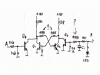
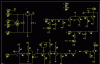
What´s the use of putting two transistor collectors shunted like the circuit in attachement! I don´t understand what this circuit does! Can anybody explain me? Thank you!
What´s the use of putting two transistor collectors shunted like the circuit in attachement! I don´t understand what this circuit does! Can anybody explain me? Thank you!
What´s the use of putting two transistor collectors shunted like the circuit in attachement! I don´t understand what this circuit does! Can anybody explain me? Thank you!
It doesn't help at all, because you've only converted the previous JPG to GIF, the JPG (as well as being far larger than a GIF) has already lost all the detail of the diagram, so converting the JPG to a GIF doesn't help at all. You need to start with a decent quality format, THEN convert it to GIF, any package should be able to generate a BMP (which is HUGE!), then convert that to GIF. I would also suggest you make the picture a bit bigger, even at good quality it's a bit small to see.
Hi,
With the bases of a few transistors being fed from a 490k to 5.6k voltage divider, the input signal must be at least 57.5V for the transistors to begin to turn on. Where is such a high voltage coming from?
I agree with Audioguru. The "490k" resistors must be much lower.
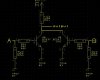
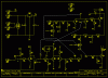
I have extracted the essential elements of the circuit and have redrawn it in a recognisable configuration. I could not read the transistor numbers, so I labelled them myself.
Q1 and Q2 are configured as a Set/Reset Flip Flop. it is set and reset by transistors Q3 and Q4.
Assume that A and B are low, and Q1 is on, therefore Q2 is off. If a high is applied to A, Q4 is turned on, but no change will occur since Q1 is on. But if a high is applied to B (with A low), Q3 will turn on, this will turn Q1 off and so Q2 will turn on.
The FF is now in its other state Q2 on Q1 off. Now if a high is applied to A (with B low), Q4 will turn on, this will turn Q2 off and so Q1 will turn on.
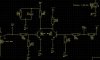
In the image i have 4 input possibilities
0 0
0 1
1 0
1 1
What´s the state of my output in each possibility?
I don´t understand if for example A=1 and B=0. With A my output=0 and for B my output=1. There´s a conflict between each transistor! It´s possible having this configuration?
Please help me... i´m confused.
This site uses cookies to help personalise content, tailor your experience and to keep you logged in if you register.
By continuing to use this site, you are consenting to our use of cookies.

")