Marks256
New Member
Ok, i built the circuit, and it works just fine. The only thing that concerns me, is the Z80 gets warm. I'm not talking really hot, just lukewarm. Is this normal? I am feeding 5 volts into it, so, what?
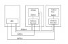
I am curious, though, what is the CPU looking for on the address bus? A0-A2 keep going up by one, then starting over? Is it looking for ROM? What can possibly be done with the numbers 0-7(%111)? I still don't understand how to address. I will draw a schematic of how i understand this will all work, then i will post it, and see what you people think. Can someone explain addressing at a scale larger than just RAM/ROM? Please? Thanks.
I am curious, though, what is the CPU looking for on the address bus? A0-A2 keep going up by one, then starting over? Is it looking for ROM? What can possibly be done with the numbers 0-7(%111)? I still don't understand how to address. I will draw a schematic of how i understand this will all work, then i will post it, and see what you people think. Can someone explain addressing at a scale larger than just RAM/ROM? Please? Thanks.

")


 I am going to order the components tomorrow(Monday). This is what i have on my list so-far(All prices are in US currency);