StopGo
New Member
I am of course over simplifying it...
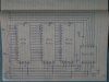
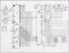
You do need to have some ROM also.
If you have a 16bit address bus.. you need to make a decision about how much ROM you need and how much RAM you need.
Normally you want lots of ROM for running programs and storing fixed data, and a small amount of RAM for variables. Maybe you need a 50/50 split though since that is simpler to understand.
You get an SRAM chip 32k x 8bit
You get a ROM chip of the same size configuration.
The address lines get connected 1:1 so.. Connect A0 - A14 on the CPU to the same pins on both the ROM and the RAM.
Now you need to resolve a possible conflict here.. you can't have the two chips using the shared wires at the same time.. so your A15 line decides which of the ROM or RAM is active at any one time.
If A15 = HIGH means the address is in the range 0x8000 to 0xFFFF
otherwise it's LOW.
So the memory chips have a /CE or "active low" chip enable. If this is LOW the chip is enabled, otherwise it switches itself off (might aswell be not there).
Connect A15 to the RAM chip CE pin.
Then take the same A15 pin on the CPU and feed it into a NOT gate (inverter) this is fed into the ROM's CE pin so the rom is active when the ram is not. This makes the ROM active in the address range where the CPU starts executing. (i think this is 0xFFF0, remeber the CE pin is "active low")
You now just need to connect up the RD / WR lines and you almost there.
Last edited:
") Then I wrote code and tested it. Finally I wrote the code to burn the EEPROM and crossed my fingers... Much easier today with a computer, compiler and burner!
Then I wrote code and tested it. Finally I wrote the code to burn the EEPROM and crossed my fingers... Much easier today with a computer, compiler and burner!  But if you don't have a burner you'll have to do what I did
  I don't recommend it.
")

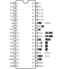
 The part number is as follows; UM61M256K-15. The reason the "M" is in bold is because it is on the chip too. They are in a 28 DIP package. Does anyone have any data on these? I suppose if you think it would be worth the effort, i will post a topic in the datasheets request forum. Thanks!
