Mike - K8LH
Well-Known Member
Ahhhh, thank you Jay... Good info'...
I use 12F683 (and other PICs) with INTOSC and MCLR disabled for I/O function and these devices will not enter High Voltage Program/Verify mode if VDD is "always on" so I definately need ICD2 controlled Target VDD functionality for programmer operation...
I also prefer P-Channel MOSFET High-Side switches in a TO-92 package but they seem to be dissappearing fast only to be replaced with much more expensive part numbers... I used to buy TP0610L in TO-92 package (very similar to BS250 or BSS84 specs') for well under $1 USD but they have become discontinued... The BSS84 is still relatively inexpensive but only comes in an SO-23 package...
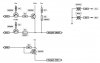
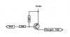
So, does your RA4 Target VDD PNP circuit look like the PNP drawing below? Do you think a 2N2907A PNP would work ok with these values to provide <100-ma to the Target?
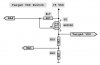
Does the drawing using a P-Channel MOSFET look ok? The low Drain-Source resistance should allow higher current to the target, yes, no?
Regards, Mike
I use 12F683 (and other PICs) with INTOSC and MCLR disabled for I/O function and these devices will not enter High Voltage Program/Verify mode if VDD is "always on" so I definately need ICD2 controlled Target VDD functionality for programmer operation...
I also prefer P-Channel MOSFET High-Side switches in a TO-92 package but they seem to be dissappearing fast only to be replaced with much more expensive part numbers... I used to buy TP0610L in TO-92 package (very similar to BS250 or BSS84 specs') for well under $1 USD but they have become discontinued... The BSS84 is still relatively inexpensive but only comes in an SO-23 package...
So, does your RA4 Target VDD PNP circuit look like the PNP drawing below? Do you think a 2N2907A PNP would work ok with these values to provide <100-ma to the Target?
Does the drawing using a P-Channel MOSFET look ok? The low Drain-Source resistance should allow higher current to the target, yes, no?
Regards, Mike
 , the thing is I learned everything without assistance of any Teacher... so there is a chance that I "see" things differently.