Continue to Site

Welcome to our site!

Electro Tech is an online community (with over 170,000 members) who enjoy talking about and building electronic circuits, projects and gadgets. To participate you need to register. Registration is free. Click here to register now.

  • Welcome to our site! Electro Tech is an online community (with over 170,000 members) who enjoy talking about and building electronic circuits, projects and gadgets. To participate you need to register. Registration is free. Click here to register now.

Understanding Optimization/Realization of the voltage controlled current source.

Status
Not open for further replies.

DX400

New Member
Hi,

I am unable to make a voltage controlled constant current source.
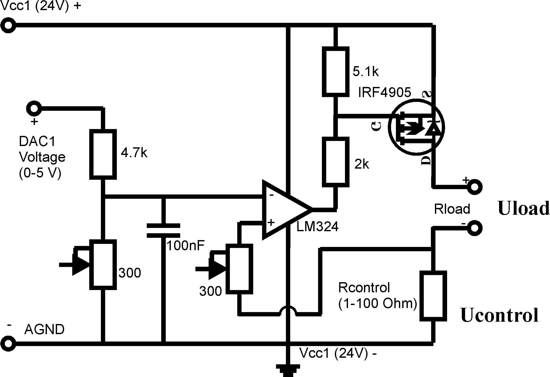
So I am using the following scheme (Sorry for bad sketch drawing):
The constant control voltage varies in the range of 0 to 5 V is applied by constant voltage supply (like HY3002 from e-bay) or (in what follows) by DAC output of PC-controlled board. So the control voltage is rather constant and linear.
The desired output parameters: constant current on load from 0.5 to 150 mA.
Sketch1.jpg

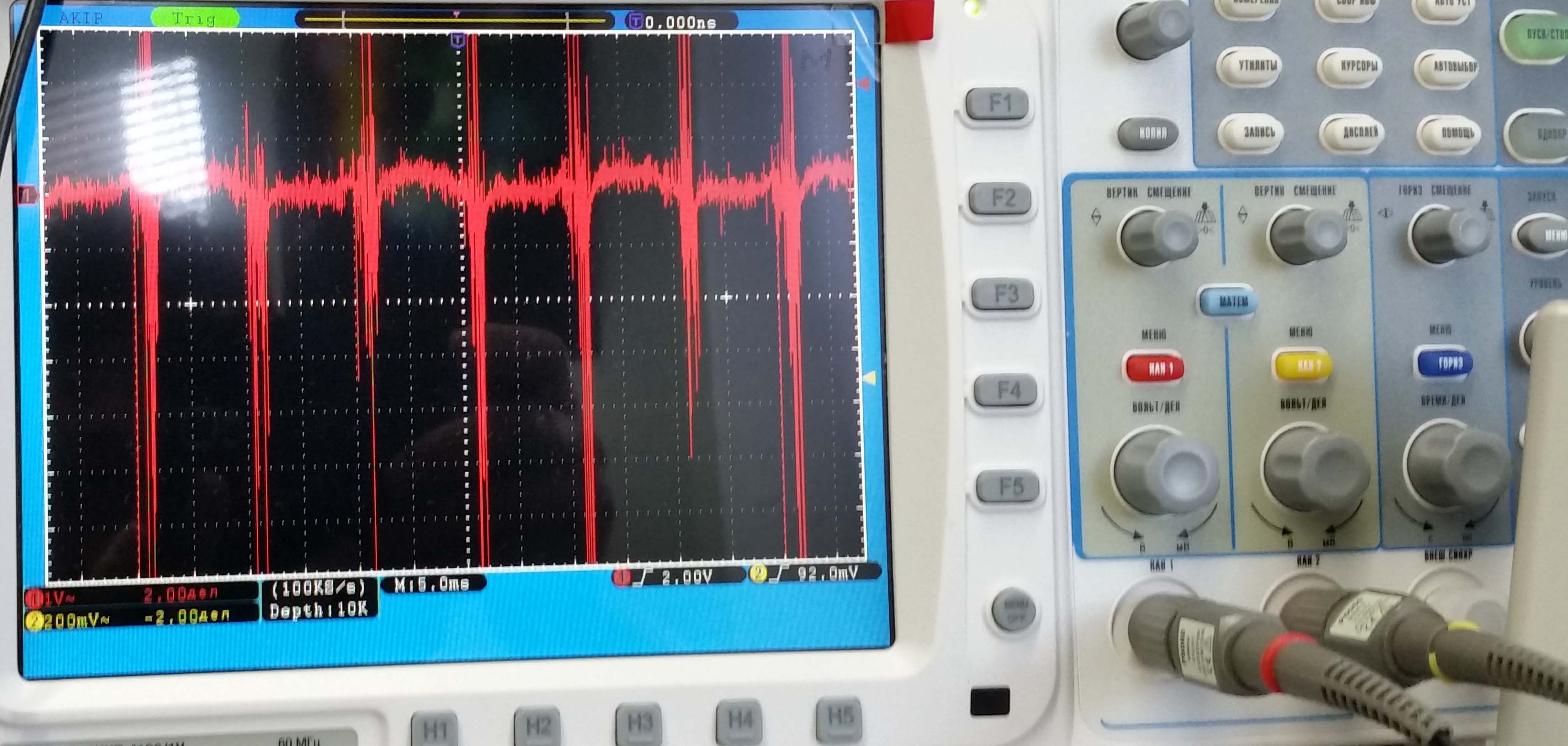
So, as a result, at the load resistance I have got the following signal.
Sketch2.jpg

The questions:
What is the source of this large noise in output signal and the signal spikes and drops?
It is possible to tune the scheme to obtain constant current or the used scheme is completely incorrect for constant current supply?
 
I suspect the opamp is oscillating doe to the delay caused be the capacitance of the FET gate.

Try adding a small capacitor between the output an negative input of the opamp; at a guess something between 10n and 100n should stabilise it.

Too small a value will not stop it oscillating, too large will make it slow to respond to load changes (of there are any).
 
the circuit is oscillating because you have positive feedback and no negative feedback. swap the inputs on the op amp.
 
An addition source of the oscillations is that the MOSFET provides added loop gain which is not compensated.
The added capacitor that rjenkinsgb mentioned should help.

What Uload do you have connected?
 
Last edited:
Here's an LTspice simulation with capacitor unconnected;
1547747328684.png
and capacitor connected:
1547747383301.png
 
It is hard to make a current source like you did. The total gain is (op-amp gain X MOSFET voltage gain). I switched to N-FET or use a npn transistor so there is no voltage gain and no inversion.
1547752576397.png

The Gate-Source max voltage should be held down. Many MOSFETs are rated for 20V and that op-amp will produce 22.5V when Rload is open so I added a resistor Zener.
 
It is hard to make a current source like you did. The total gain is (op-amp gain X MOSFET voltage gain). I switched to N-FET or use a npn transistor so there is no voltage gain and no inversion.
View attachment 116188
The Gate-Source max voltage should be held down. Many MOSFETs are rated for 20V and that op-amp will produce 22.5V when Rload is open so I added a resistor Zener.
I made one of those for work but it blows all the time and is really finnicky (we are driving a waveform through an inductor though). Not sure of a better way to do it though.
 
I made one of those for work but it blows all the time and is really finnicky (we are driving a waveform through an inductor though). Not sure of a better way to do it though.
Send a schematic with load. "through an inductor" Details on load. It is common for an inductive load to blow up current sources.
 
Hello,

Yes the problem with a PNP or PMOS output stage is the gain goes up a lot and then the op amp is no longer properly compensated.

The cap from output to inverting input helps. You do have to check it carefully though unless you are willing to do a full analysis. A full analysis would mean something like a root locus plot.
You also have to be careful with different types of loads like capacitive and inductive. It may be stable for resistive and then not for cap or inductive. Very careful testing is in order and possibly a root locus with a range of loads instead of a range of gains.

Using the N channel NMOS or NPN works easier because there's no additional gain. The only loss there then is the NMOS turn on voltage drop or the NPN base emitter drop and because you cant always get away with just one NPN you might see two base emitter drops with two NPN's.
This can be significant when using a standard NMOS as the turn on voltage might he as high as 10v. With two NPN's it could be as high as 2 or 3 volts depending on choice of transistor.
 
Send a schematic with load. "through an inductor" Details on load. It is common for an inductive load to blow up current sources.
ditto... if you use bipolar transistors, driving an inductive load can take the transistor into its secondary breakdown region, and the transistor instantaneously self destructs. using a MOSFET, you can easily go past the Vgs breakdown voltage limit. because of the phase shift, inductive and capacitive loads will have the voltage and current out of phase, which if not compensated for will cause oscillation.
 
Hello,

Yes the problem with a PNP or PMOS output stage is the gain goes up a lot and then the op amp is no longer properly compensated.

The cap from output to inverting input helps. You do have to check it carefully though unless you are willing to do a full analysis. A full analysis would mean something like a root locus plot.
You also have to be careful with different types of loads like capacitive and inductive. It may be stable for resistive and then not for cap or inductive. Very careful testing is in order and possibly a root locus with a range of loads instead of a range of gains.

Using the N channel NMOS or NPN works easier because there's no additional gain. The only loss there then is the NMOS turn on voltage drop or the NPN base emitter drop and because you cant always get away with just one NPN you might see two base emitter drops with two NPN's.
This can be significant when using a standard NMOS as the turn on voltage might he as high as 10v. With two NPN's it could be as high as 2 or 3 volts depending on choice of transistor.

Yeah, I think stability was definitely an issue. I've had a few versions of the circuit and some worked better than others. The one that worked best used just an LTC6090 driving a linear-optimized power NMOS + heatsink block (not shown but was basically the circuit below without the power op-amp in the middle).

Unlike the schematic shown, it used multiple LTC6090 in parallel with thermal shutdown enabled but in the LTC6090 was very prone to overheating and dying. So I added in a heatsinked power-op amp to get the circuit below and it became even more finicky. The negative power-rail of the circuit got blown while I was trying to get it to work so it has a offset now and haven't replaced the power-amp because it's like $130. Super finicky and really noisy. You can practically see the control loop trying to do its thing looking at the waveform.

1547788649248.png


Don't want to hijack this thread though.
 
Last edited:
Yeah, I think stability was definitely an issue. I've had a few versions of the circuit and some worked better than others. The one that worked best used just an LTC6090 driving a linear-optimized power NMOS + heatsink block (not shown but was basically the circuit below without the power op-amp in the middle).

Unlike the schematic shown, it used multiple LTC6090 in parallel with thermal shutdown enabled but in the LTC6090 was very prone to overheating and dying. So I added in a heatsinked power-op amp to get the circuit below and it became even more finicky. The negative power-rail of the circuit got blown while I was trying to get it to work so it has a offset now and haven't replaced the power-amp because it's like $130. Super finicky and really noisy. You can practically see the control loop trying to do its thing looking at the waveform.

View attachment 116193

Don't want to hijack this thread though.

Hi,

Looks like the inductor could use some back emf clamping. It's a boost converter with no load in one operational mode :)
 
Schematic in post #12; why a power amp to drive a Gate? Why +50 volts and -24 volts to drive the gate. If the load is removed the mosfet dies. Quickly removing the current kills the fet. The power driver is hot because of oscillation. Two amps?
 
Hi,

Looks like the inductor could use some back emf clamping. It's a boost converter with no load in one operational mode :)
The actual circuit has TVS diodes across the power NMOS, amp, but not across the inductor because it was physically impractical without really long lead wires. Otherwise, yeah, the circuit would have blown from voltage spikes long ago.

Schematic in post #12; why a power amp to drive a Gate? Why +50 volts and -24 volts to drive the gate. If the load is removed the mosfet dies. Quickly removing the current kills the fet. The power driver is hot because of oscillation. Two amps?

The -24V could have been a lot less but was the most convenient supply I had and is just there to provide a little negative supply since I needed to work close to 0V but the LTC6090 is not a rail-to-rail op amp.

50V is what was required to produce the necessary slopes to produce the current waveforms we wanted in the inductor. THe LTC6090 is powered off 50V so it can accept the worst case current sense voltage even though it never actually outputs that during normal operation, resulting in a volt of voltage drop across it, which I think was the reason it overheated.

The power NMOS was a IXYS IXTN200N10L2
https://ixapps.ixys.com/DataSheet/DS100238(IXTN200N10L2).pdf

The power-amp was an Apex PB58:
https://www.apexanalog.com/resources/products/pb58u.pdf

Now that I type this out, I realize some details were left out. The actual setup has six power NMOSs in parallel which I forgot to put into the simulation schematic above. I need to add that.

Note that in all this, there were TWO versions of the circuit. The schematic shown in is the SECOND version (but omits the six parallel power NMOSs which the actual circuit has).

The first circuit is essentially the same thing, but without the power-amp in the output path of the LTC6090 wired as a unity buffer, and with four LTC6090s in parallel. This circuit was less finicky than the one containing the power-amp but suffered from the LTC6090s overheating. The second circuit with the power-amp (aka the schematic above) did not overheat but was even more finicky.

You mention oscillations. Are you referring to oscillations due to instability? Or just the regular oscillating nature of the signals coming from our source signal? Because whenever the LTC6090s circuits died due to heat it was stable (or maybe only marginal stable, since as I previously mentioned, there was a lot of noise riding on the waveform. It almost looked like it wasn't noise but was the control loop visibly fighting to keep the circuit under control). This "noise" was present in both versions of the circuit.
 
Last edited:
The actual circuit has TVS diodes across the power NMOS, amp, but not across the inductor because it was physically impractical without really long lead wires. Otherwise, yeah, the circuit would have blown from voltage spikes long ago.
<snip>
.

Hi,

I thought there might have been something else there too or else it would have blown out every time :)
Thought i would mention it anyway.
 
Status
Not open for further replies.

Latest threads

New Articles From Microcontroller Tips

Back
Top