Continue to Site

Welcome to our site!

Electro Tech is an online community (with over 170,000 members) who enjoy talking about and building electronic circuits, projects and gadgets. To participate you need to register. Registration is free. Click here to register now.

  • Welcome to our site! Electro Tech is an online community (with over 170,000 members) who enjoy talking about and building electronic circuits, projects and gadgets. To participate you need to register. Registration is free. Click here to register now.

Understanding a well designed FM Transmitter - AudioGuru's MOD4

Status
Not open for further replies.

KamalS

New Member
I stumbled across AudioGuru's MOD4 by chance when answering a forum question and I really like the features it has:

1. PreEmphasis (nice for speech and audio transmission)
2. Regulated power supply for the oscillator so that freq. does not destabilize because of changing voltage
3. Isolating RF amplifier that not only boosts the power of the Tx but isolates the antenna as well. The better thing is that this portion works off the unregulated voltage and thus you get the whole battery power as output.

There are a few disadvantages as well:

1. It is after all, a LC oscillator (the LC tuner will give a theoretical range of 87 - 185Mhz)
Temperature, humidity changes and parasitic capacitance WILL affect it.
2. The freq. response to the modulating signal is not flat from DC to 60Khz (required for stereo encoding)
3. It seems the final stage consisting of C13 and L2 can be dropped with only the range of the circuit getting affected?
4. Maybe we can replace the LDO with a less expensive (cost, space and need for extra caps) 5v1 zener diode?
5. Q2 can be replaced with a Zener, say 16V (zeners have better response as a varcap than the BE of a transistor)

Now I am far from a person knowledgeable in RF, and that is why I am asking you guys for help, but I would like to begin with a stage by stage explanation (as far as I understand) of how the circuit operates.

I will keep on modifying this explanation as I get more experts to contribute, and be the the hope that we can make this better (maybe get a more stable freq. response? Maybe a Vackar oscillator someone?)

I have done a trivial modification to start with - changed R1 to 4K7 and C1 to 10nF

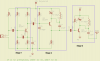
Next comes the 3 stages:

Stage 1:

This only serves to amplify the AC signal from the electret (DC bias filtered out by 10n) - Freq less than X kHz are attenuated by C1

1. R2 + R3 form a divider network that adds a ~0.8v offset to this signal?
2. C2 + R5 + C4 forms a RC filter?
3. How is the transistor kept in its active region in this stage?

The output of this stage is AC coupled to stage 2 via C3. Freq less than Y kHz are attenuated by C3

Stage 2:

This seems to be a complex RCL tuner circuit.

4. R6 supplies (5 / 47) = 0.106mA to the base of Q2.
5. The collector is connected directly to 5v (via L1) and could have sank upto (5 - Vfe / 220) ~ 20mA current
6. Keeping point 4 at mind, this implies that Q2 is also not in saturation and thus its BE junction can be modulated
7. The output of this stage is AC coupled to stage 3 via C12. Freq less than Z kHz are attenuated by C12
8. I am not sure what C5 does

As you can see, I am not sure how Stage 2 works out, and I need help on this of course.

Stage 3:

This seems to be a copy of stage 2.

Possible reasons are to:

9. isolate the antenna from the oscillaor circuit
10. provide amplification (both by the BJT as well as resonance) to the RF signal from C12
11. It goes without saying that the Carrier freq chosen at stage 2 should be mirrored here exactly
12. You can do away with C13 and L2 and only reduce the range/output power of the Tx without affecting it in any other way?

This is a nice Tx speech and mono audio transmission, and by making the oscillator stable (XTAL/vacar), it can be made to work more reliably.

Somebody care to do a TINA (or better?) simulation to see how things work out?
 

Attachments

  • sch.processed.png
    sch.processed.png
    13.1 KB · Views: 506
C1 passes audio frequencies down to about 30Hz to the RF oscillator. You increased its value 33 times so it will not pass frequencies below 990Hz and will sound very tinny.

Q1 uses the emitter resistor R5 to stabilize its operating point if the transistor has higher or lower DC gain or if its gain is affected by temperature changes. When something causes the transistor to try to conduct more then it draws more current in the emitter resistor that increases the emitter voltage that reduces the increase in the transistor's current. It also does the opposite if the transistor tries to conduct less. R5 is also part of the pre-emphasis boosted high audio frequencies.

Q2 is a radio frequency oscillator. It is tuned with L1 and C6, the capacitance of Q2, C7 and stray capacitance. C7 provides positive feedback for oscillation to be continuous.
Q2 is a common base amplifier with C5 grounding its base at radio frequencies. Audio modulation to the base of the transistor causes its current to change which causes its capacitance to change which causes its frequency to change producing FM.

Q3 keeps the RF oscillator frequency from changing if something moves toward or away from the antenna. It also increases the range.
C13 and L2 filter the RF output so even if the crudely biased Q3 clips, the output does not have many harmonics to cause interference to other communications. when C13 and L2 are peaked at 98MHz then they still pass 88MHz and 108MHz pretty well.
 
Bit of constructive criticism:

1. You appear to have forgotten the RF decoupling from +5 to ground. When this basic circuit appeared in the 1970's, "R6" was bypassed with 470pF to provide this.

2. To save parts you can delete C3, R6 & C5, then connect Q2 base to Q1 collector.

3. Efficiency can be optimised by operating Q3 in class b (edit: it is already).

4. There is no 2nd & 3rd harmonic filter before the antenna, this would need adding the TX gave interference to higher frequency users.

5. Output power can be increased for short antennas by adding an inductor as a "loading coil"

Overall, well done, it's nice to see this circuit is still alive and well, and still evolving.
 
Last edited:
When this basic circuit appeared in the 1970's, "R6" was bypassed with 470pF to provide this.
That's C5's job.
3. Efficiency can be optimised by operating Q3 in class b.
It already is nearly operating in class B, the current goes down to near 0.
 
Last edited:
That's C5's job.

Then how does C5 couple RF from top end of L1/C6 to ground?

In RF circuits, one needs a return path for RF currents, especially harmonics. Otherwise they'll go where they're not wanted, i.e. disrupt other circuits. (luckily, this is a simple circuit and has no 'other circuits')

Complete RF decoupling of this oscillator I would of thought even more important, since this design is particularly prone to frequency drift, especially with variations in ambient temperature.

...which draws me to look a bit further. Another improvement to the design is to make C7 a 10 pF trimmer. That should* allow a little more RF output power to be found, without adding another transistor.

* I can't promise anything, but in my experience it improves.
 
Last edited:
Are you talking about adding a capacitor across the supply rails?

That isn't what you said, you just said bypass R6 with 470pF.
 
Are you talking about adding a capacitor across the supply rails?

That isn't what you said, you just said bypass R6 with 470pF.

Same difference, as far as RF return path coupling is concerned.

In 1970's when I first saw this circuit, "R6" was RF bypassed. In 'grounded-base' circuits, each supply rail tends to be AC-coupled to the base.

.... oh, and another improvement I can see, is if a 1/4 wave antenna is used, it can be better matched by attaching it to a tapping on L2
 
Last edited:
It doesn't make any difference whether C5 goes to +5V (what you're suggesting or 0V (how it currently is).
 
It doesn't make any difference whether C5 goes to +5V (what you're suggesting or 0V (how it currently is).

Then how can C5 couple RF from the top end of L1/C6 back to ground? Couple this RF around the power rails?


oh.... and another improvement in the circuit (reduction of parts count) is to discard C1, R1 & R2, then connect the electret microphone in place of R2, and reduce the value of R3 to restore the DC bias point.
 
Last edited:
It doesn't make any difference whether C5 goes to +5V (what you're suggesting or 0V (how it currently is).

That wasn't what he meant, he actually explained VERY poorly what he meant.

He was referring to a power suply decoupling capacitor, from the TOP of R6 down to ground - an absolutely essential component.

However, feeling charitable, I presumed it wasn't shown because the 5V regulator isn't shown either, and it's probably drawn on that missing part of the circuit.

Well in that case the 'missing part of the circuit' has been repeated several times. In RF circuits, each stage has local supply rail decoupling. This circuit shows none.

.... that's another improvement on the circuit by the way (stability, less parasitic oscillation): Add supply decoupling capacitors to each Stage.
 
Very nice. Decoupling capacitors are obviously important, and I have not added any (in the final schematic, I would connect 0.1uF ceramics for power supply).

Should I also add some 470pF from +5 to GND for RF decoupling? I am not sure here.

What I am interested in right now are:

1. Values of X, Y, Z Khz in my original posting (and how to calculate values of coupling capacitors - these caps seem to be simple high pass filters?)

2. More details on how Q1 uses the emitter resistor R5 to stabilize its operating point

3. More details on how Q2 can behave like a radio frequency oscillator

4. Why is Q3 said to be crudely biased?

5. Are not Stage 2 and 3 the same (expect a feedback oscillator is not there any more in stage 3 unlike stage 2, but the oscillations are already underway)?

6. I am also confused by marcbarker's comments :

a. To save parts you can delete C3, R6 & C5, then connect Q2 base to Q1 collector.
b. discard C1, R1 & R2, then connect the electret microphone in place of R2, and reduce the value of R3 to restore the DC bias point.

For tip a - what freq does C3 pass and attenuate?
If I remove C5, will not RF swamp the circuit more, as C5 seems to be the return path?

For tip b - I am sure the circuit will stop functioning correctly as the electret would now have no bias at all, and thus provide no output.

Thanks all for the detailed answers!
 
Very nice. Decoupling capacitors are obviously important, and I have not added any (in the final schematic, I would connect 0.1uF ceramics for power supply).

Should I also add some 470pF from +5 to GND for RF decoupling? I am not sure here.
A 0.1uF ceramic capacitor might be inductive at 100MHz. I used 1000pF for a good RF bypass.

1. Values of X, Y, Z Khz in my original posting (and how to calculate values of coupling capacitors - these caps seem to be simple high pass filters?)
The calculation for the value of a coupling capacitor is 1 divided by 2 pi x the frequency x the resistance it comes from plus the resistance it drives.

2. More details on how Q1 uses the emitter resistor R5 to stabilize its operating point.
It is standard DC negative feedback. a transistor has a range of spec's and DC negative feedback cancels the differences.

3. More details on how Q2 can behave like a radio frequency oscillator.
It is a form of Colpitts oscillator.

4. Why is Q3 said to be crudely biased?
Because a linear transistor should never be biased from the supply with a single resistor. If the transistor has high hFE then it will be saturated. If the transistor has low hFE then it is almost cutoff.
In this simple circuit the tuned circuit of C13 and L2 smooths the sine-wave even if Q3 is biased wrong and is clipping.

5. Are not Stage 2 and 3 the same (expect a feedback oscillator is not there any more in stage 3 unlike stage 2, but the oscillations are already underway)?
No.
The RF input for Q2 is its emitter.
The RF input for Q3 is its base.

6. I am also confused by marcbarker's comments :

a. To save parts you can delete C3, R6 & C5, then connect Q2 base to Q1 collector.
b. discard C1, R1 & R2, then connect the electret microphone in place of R2, and reduce the value of R3 to restore the DC bias point.
I disagree.
I use 5% resistors to bias Q1 where it is supposed to be biased. But the current in an electret mic has no tolerance.

For tip a - what freq does C3 pass and attenuate?
C3 passes audio frequencies above its calculated cutoff frequency.
It reduces the level of frequencies below its cutoff frequency.

If I remove C5, will not RF swamp the circuit more, as C5 seems to be the return path?
C5 grounds the base of Q2 at RF frequencies so that it can be a common-base oscillator.

For tip b - I am sure the circuit will stop functioning correctly as the electret would now have no bias at all, and thus provide no output.
The current into R3 and in the base of Q1 would flow in the mic. But the current of an electret mic has no minimum and no maximum so its tolerance would stop Q1 from amplifying.
 
a. To save parts you can delete C3, R6 & C5, then connect Q2 base to Q1 collector.
b. discard C1, R1 & R2, then connect the electret microphone in place of R2, and reduce the value of R3 to restore the DC bias point.

For tip a - what freq does C3 pass and attenuate?
If I remove C5, will not RF swamp the circuit more, as C5 seems to be the return path?

For tip b - I am sure the circuit will stop functioning correctly as the electret would now have no bias at all, and thus provide no output.

C3 is presently used for: 1. DC level shift, & 2. (potentially) as 'bass cut' function to exclude wind noise if later developed.

C5 is not the only RF return path. The RF return path from top of L1 is presently via the supply rails, which has been described as 'wrong'. I don't believe anyone was ever suggesting removing C5. If anything "supply rail decoupling" is missing. I am saying that in the 1970's form of this circuit, "R6" also had a 470pF bypassing it, this provided RF return path from the top of L1. In the 70's the expertise in transistor circuit design was not 'diluted' as it is today. Nowdays the trend is to sprinkle decoupling capacitors everywhere and hope one doesn't go short circuit.

a. When I tried it worked. Q2 base needs to be RF bypassed to ground, and moreorless held steady (and waggled to modulate it). Q1 collector does this already, the only thing that is a weakness is Q2 base wants to be a lower voltage than Q1 collector (presently about 2.5 V). You'd need to get the collector voltage lower by re-biasing it. You can have your cake and eat it by making Q1 a PNP instead (inverting stage 1 circuit), this will allow a lower base voltage to be used on Q2.

In b. the electret is considered a replacement for R2. The bias voltage for the electret is Vcc minus Q1's base voltage. Roughly 4 V. R3 would need to be changed in value to reset the bias of Q1. Since Stage 1 contains a good measure of DC negative feedback, variations of the electret DC resistance are tolerated.
 
Last edited:
marc, thanks for your comments!

I have been noticing that you mention a 1970 version of the circuit. I am sure there were matured Colpitts by then, so can you trace out a variant of the circuit that closely resembles what you are talking about?
 
Last edited:
marc, thanks for your comments!

I have been noticing that you mention a 1970 version of the circuit. I am sure there were matured Colpitts by then, so can you trace out a variant of the circuit that closely resembles what you are talking about?

Somewhere, I think in loft, I have a very yellow-looking A4 sheet with the 1970's circuit. I purchased it as a kit mail order in 1979. The circuit is very similar, it used a 2N2222 too.

For 100 MHz the grounded-base configuration is often used. For lower frequencies, it's like the class-c oscillator from Denver Uni that I'd posted above.
 
Last edited:
For a frequency as low as you want, the antenna for the transmitter and radio should be a few km long.
If you try to FM modulate your low frequency by varying the very small capacitance of the transistor then the modulation will be almost nothing.
 
My freind transmits on 80 kHz (VLF station), with 100 mW or something, heard all over Europe. I think his antenna is less than a kilometer though.
 
Last edited:
Status
Not open for further replies.

Latest threads

New Articles From Microcontroller Tips

Back
Top