Continue to Site

Welcome to our site!

Electro Tech is an online community (with over 170,000 members) who enjoy talking about and building electronic circuits, projects and gadgets. To participate you need to register. Registration is free. Click here to register now.

  • Welcome to our site! Electro Tech is an online community (with over 170,000 members) who enjoy talking about and building electronic circuits, projects and gadgets. To participate you need to register. Registration is free. Click here to register now.

troubleshotting a counter

Status
Not open for further replies.

PG1995

Active Member
Hi,

Please have a look here. Could you please help me with the query?

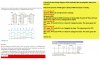
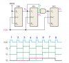
It is said that the AND gate has a fault and its lower input, i.e. #2 input, is always HIGH internally.

It means the output of AND gate is controlled by upper input, i.e. #1, and input comes from Q0.

When Q0 is HIGH, the output Q2 of rightmost flip flop, FF2 (EDIT: it was written FF3 previously), toggles. When Q0 is LOW, FF3 gets RESET. But this is not what happening when you look at the waveform. For example, at "X", Q0 is LOW but Q2 is still HIGH. Could you please help me?

Thank you!
 

Attachments

  • COUNTER_troubleShooting.jpg
    COUNTER_troubleShooting.jpg
    271 KB · Views: 218
Last edited:
The clock inputs are positive edge triggered.

That means state changes occur then the clock line rises and only it is only at that instant the data inputs are important.

In reality the clock waveform would be advanced from Q vareforms by a tiny amount, probably some nanoseconds depending on the logic family in use.

The output changes take place a short sime after the clock edge, so only matter at the following clock.
 
Thank you but I'm still confused.

I understand that the propagation delays make the outputs of flips flops and other components lag behind with reference to clock pulse by some nanoseconds.

The book is ignoring propagation delays for that example, and even if we assume propagation delays which would mean that the change occurs for point X at clock pulse #3 instead of #2, the output Q2 of FF2 is still wrong, in my opinion. Thank you.
 
It looks to be correct.
A JK flip flop changes state on the clock edge if both inputs are high, or holds its state if they are both low.

At each clock where Q0 was high, Q1 and Q2 both change state. That matches the idea that only input 1 of the AND gate is working as with that both FF1 and FF2 get the same input levels.

If they were eg. D type flip flops, the operation would be totally different.
 
Thank you for your help.

It makes sense now. You can have a look here.

It looks like the timing diagram does implicitly take propagation delay into account.

Note that input #2 of AND gate is always HIGH because it's faulty.

Clock pulse #1:
Q0 goes HIGH. Q1 and Q2 doesn't change.
Clock pulse #2:
Q0 goes LOW.
Q1 and Q2 both goes HIGH because at rising edge of pulse #2 they still saw HIGH level of Q0 so they changed their states.
Clock pulse #3:
FF1 sees J1=0 and K1=0 so it doesn't change its state. The same goes for FF2.
Clock pulse #4:
FF1 sees J1=1 and K1=1 so it toggles its state. The same goes for FF2.
Clock pulse #5:
FF1 sees J1=0 and K1=0 so it doesn't change its state. The same goes for FF2.

and so on.

faulty_and_gate-jpg.117757
 

Attachments

  • COUNTER_troubleShooting_new.jpg
    COUNTER_troubleShooting_new.jpg
    322.5 KB · Views: 210
  • faulty_AND_gate.jpg
    faulty_AND_gate.jpg
    34 KB · Views: 194
Status
Not open for further replies.

Latest threads

New Articles From Microcontroller Tips

Back
Top