Continue to Site

Welcome to our site!

Electro Tech is an online community (with over 170,000 members) who enjoy talking about and building electronic circuits, projects and gadgets. To participate you need to register. Registration is free. Click here to register now.

  • Welcome to our site! Electro Tech is an online community (with over 170,000 members) who enjoy talking about and building electronic circuits, projects and gadgets. To participate you need to register. Registration is free. Click here to register now.

Transistor circuit help ?

Status
Not open for further replies.

tron87

New Member
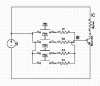
How do i calculate the IB and resistance values of r1,r2,r3,r4 required to do the following to the collector current when each pushbutton is pressed in turn:

1.When pb1 is pressed transistor is fully saturated and near 1 amp flows on Ic ?


2.When pb4 is pressed transistor operates in active region and makes Ic = 500ma ?


3.When pb3 is pressed transistor operates in active region and makes Ic = 10ma ?


4.When pb2 is pressed transistor operates in active region and makes Ic = 0.1ua ?


The transistor is a Bc548A npn bjt the circuit is purely just to learn about a transistor active region and how to calculate required biasing current.


*Circuit diagram is attached*
 

Attachments

  • transistor active region.JPG
    transistor active region.JPG
    550.4 KB · Views: 443
Last edited:
The circuit you have shown is very dependent on the current gain Hfe of the transistor; this is an unknown and variable value. To provide a better solution, negative feedback needs to be used by way of either an emitter resistor or a resistor between the collector and base.
 
Hi,

You are learning how to bias a transistor.

Here is 2 examples of how to practice biasing a transistor.

First into its saturation region.

Refer to the data sheet, given below.


DATA SHEET
--------------
bc548 data.jpg


Saturation design.
---------------
base current saturation.jpg

Now how to use the same value for RC, but put the transistor into its linear region.

Linear design
----------------
base current linear.jpg

These are very basic ways of designing this.

There is a lot more detail involved but this should give you some practice, on biasing transistors.

Experiment with different values, to see how it works out.
 
Thanks JCLrd for taking time to explain !

Question though what does ID mean in your design examples ?
 
Last edited:
Thanks JCLrd for taking time to explain !

Question though what does ID mean in your design examples ?

ID = Icurrent thru the Divider
The divider is the two resistors to the transistor base.
Usually you calculate ID to be 10 times Ib
 
The BC547 transistor you selected has a max allowed collector current of only 100mA.
It is very difficult to see the numbers on your small and negative schematic but it looks like a 10V supply and a collector resistor of only 10 ohms.
Ohm's Law calculates the saturated collector current to be almost 1A which will blow up the transistor.

I made your awful schematic a normal positive image and removed the pastel colours.
I couldn't remove the chicken-pox dots all over it.
 

Attachments

  • transistor.PNG
    transistor.PNG
    62.2 KB · Views: 130
Status
Not open for further replies.

Latest threads

New Articles From Microcontroller Tips

Back
Top