PG1995
Active Member
Hi,
Could you please help me with the queries below? Thank you.
Question 1:
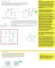
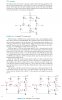
I believe that the words pull-up/pull-up network and push-pull network are synonymous in the context of circuits.
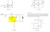
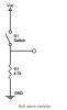
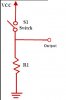
It is my understanding that when the word pull-up/pull-down is used, it refers to combination of a resistor and switch such as this one. Such a combination is used to pull the output voltage toward ground or toward the supply voltage; in other words low and high.
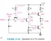
The totem-pole circuit also does the same thing, in my opinion, making the output low or high but its use is mostly restricted to turning on/off of FET transistors.
You can see here four circuits and all of them look different from each other considering the layout of components but function-wise they are pretty much the same in the context of given circuit.
Do I have it correct?
Sources:
Circuit #1 and #2 were taken from this webpage.
Circuit #3 is from an MPPT circuit.
Circuit #4 was taken from here.
Please have a look here.
Question 2:
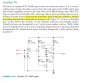
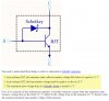
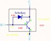
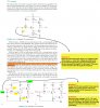
Does this mean that when there is a negative spike at the input, i.e. when the voltage goes below the ground level temporarily, the current flows from ground terminal through D1 to the input? This way current wouldn't flow through Q1 transistor.
Question 3:
It says Vcc=5V but wouldn't it then require HIGH to be greater than 5V if the base emitter junction of Q1 transistor is to be reverse biased.
Question 4:
How are these voltages, 2.1V, 1.4V, and 0.7V calculated? They add up to 4.2V and not to 5V. Perhaps, the author is just trying clarify a point without making an exact calculation.
Thanks a lot!
Could you please help me with the queries below? Thank you.
Question 1:
I believe that the words pull-up/pull-up network and push-pull network are synonymous in the context of circuits.
It is my understanding that when the word pull-up/pull-down is used, it refers to combination of a resistor and switch such as this one. Such a combination is used to pull the output voltage toward ground or toward the supply voltage; in other words low and high.
The totem-pole circuit also does the same thing, in my opinion, making the output low or high but its use is mostly restricted to turning on/off of FET transistors.
You can see here four circuits and all of them look different from each other considering the layout of components but function-wise they are pretty much the same in the context of given circuit.
Do I have it correct?
Sources:
Circuit #1 and #2 were taken from this webpage.
Circuit #3 is from an MPPT circuit.
Circuit #4 was taken from here.
Please have a look here.
Question 2:
Does this mean that when there is a negative spike at the input, i.e. when the voltage goes below the ground level temporarily, the current flows from ground terminal through D1 to the input? This way current wouldn't flow through Q1 transistor.
Question 3:
It says Vcc=5V but wouldn't it then require HIGH to be greater than 5V if the base emitter junction of Q1 transistor is to be reverse biased.
Question 4:
How are these voltages, 2.1V, 1.4V, and 0.7V calculated? They add up to 4.2V and not to 5V. Perhaps, the author is just trying clarify a point without making an exact calculation.
Thanks a lot!
Attachments
Last edited: