Continue to Site

Welcome to our site!

Electro Tech is an online community (with over 170,000 members) who enjoy talking about and building electronic circuits, projects and gadgets. To participate you need to register. Registration is free. Click here to register now.

  • Welcome to our site! Electro Tech is an online community (with over 170,000 members) who enjoy talking about and building electronic circuits, projects and gadgets. To participate you need to register. Registration is free. Click here to register now.

timed gated circuit

Status
Not open for further replies.

earckens

Member
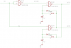
A circuit needs to be triggered by one input, resulting in two outputs as follows and with following conditions:
1. 0 = 0V, 1 = 5V
2. OUT1 and OUT2 may never be 0 at the same time
3. the input signal must trigger state transitions for OUT1 and OUT2 (see points 4 and 5)
4. when OUT1 goes to 1, a fixed time T1 later OUT2 goes to 0
5. when OUT2 goes to 1, a fixed time T1 later OUT1 goes to 0

OUT1: 1 1 0 0 1 1 1 1 0 0.....
OUT2: 0 1 1 1 1 0 0 1 1 1 ...

So OUT1 and OUT2 must overlap in the status 1 during T1

How can this be solved with hardware?
 
I'd start with an inverter, to take the single "master control" signal, whatever you want to call it, and create an inverse of that as well.

Then two identical output circuits with an instant-on and delayed-off function.

They could be eg. an OR gate with one input direct from the appropriate control signal and the other input via a resistor capacitor diode type delay from the first input.
(ie. capacitor on the second input, charged via a lowish value resistor and diode from the first input when the signal goes high, discharged via a higher value resistor when the first input goes low).

Two of those, one on each the signal in & out of the inverter.

At each input change, the new output becomes active instantly and the old output "holds on" for whatever time is set by the capacitor on the second OR gate input discharging.
Would something like this do it? I checked and think it would, but I'd rather check with you:

1542371977162.png
 

Attachments

  • 1542371840939.png
    1542371840939.png
    10.1 KB · Views: 87
Yep, that's using negative logic for the "or" function but should work just the same - plus the advantage of the schmitt trigger gate inputs.

I'd connect the RC circuit input just to the other input of the same gate, rather than the opposite output, but it will probably not make much difference.

Either way, add a resistor in series with the diode as otherwise the signal feeding that will be delayed by the capacitor charge (or discharge) current; eg. 4k7

You could also use rather higher value timing resistors and smaller caps, on the CMOS inputs. Something in the 100K to 1M should be fine. eg. 470K and 1uF would give the same time constant.
That minimises the charge time through the diode and its resistor while still allowing a long off delay if needed.
Great, thanks for your input! I keep you posted with oscilloscope readings of the result.
Is the use of out1 to in2, out2 to in1, not a safer way to obtain the desired result: interlocking?
 
Status
Not open for further replies.

Latest threads

New Articles From Microcontroller Tips

Back
Top