Continue to Site

Welcome to our site!

Electro Tech is an online community (with over 170,000 members) who enjoy talking about and building electronic circuits, projects and gadgets. To participate you need to register. Registration is free. Click here to register now.

  • Welcome to our site! Electro Tech is an online community (with over 170,000 members) who enjoy talking about and building electronic circuits, projects and gadgets. To participate you need to register. Registration is free. Click here to register now.

Still Struggling with my 1st PCB toner transfer

Status
Not open for further replies.
It seem to recall that people are doing finer traces with pulsar then P&P not sure.

From the pulsar site

Now using any standard 1200 dpi laser printer and the TIA applicator, you can image down to .006" (and below!) We've had customers who have reported traces down to .004"!
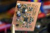
As I pointed out earlier I am not a huge fan of using fine lines if I do not have too. I would rather go with stuff that I know will work 100% of the time. As the lines get narrower it gets harder to detect break with the naked eye.

Just because you can does not mean you should.
 
I use magazine paper because

1) It's free
2) I can get 10 mil traces and no errors.
3) I tend to like the flexibility of always having paper on hand.

When I first started, I had a few flaws or gaps in the artwork. Shorts don't really happen. The soak and peel process is 20 min extra but it's not like u have to stare at it. You can do sumthin else while it soaks, like put away the iron/laminator, or setup your drill press or pick the parts from your stock or go feed the dogs etc.

I have NEVER used bought paper. I am sure it does what it claims. The magazine paper approach takes a bit more skill & patience, but once u have the skill it's nothing special. Folks on the US mainland etc. tend to go for the convenience items. If a pack of paper costs u 15 USD. It costs me 30USD. If it takes 2 days to get it, it takes 8 days for me. As such I prefer to be self sufficient wherever possible. Especially for consumables.

U guys might think it's funny but I still have some circuits that were built as follows:

I had no access to Ferric Chloride, Resist ink, Raw PCB boards, but I wanted to make PCB circuits. I had to be creative.

1) On your stove, make a lead plate 6 " X 6" from melted car battery plates. (reusable - only do this once)
2) Electroplate copper sulphate solution with copper coin anodes to make copper foil onto the Lead plate. (Overnight)
3) Peel the foil & GLUE it onto Arborite laminate.
4) Use a Calligraphy pen heated by wrapped enamelled transformer wire & driven by a 12VDC adapter.
6) Dip the Pen into coloured vaseline and hand draw the resist lines onto the copper.
7) Etch in Nitric Acid.


That was a long time ago when I was 16 yrs old and had no $$ to buy much except the components. Plus the hobby stuff was less common and much more expensive....no internet competition.

For prototypes etc the mag paper is fine, or use Pulsar paper if u have it. For production send out to a PCB facility.
 
Last edited:
Ok I went the office and with the help of my wife I managed to print out and transfer 5 boards in a half hour with pages out of a magazine. The magazine turned out to be not so good of quality and some of the paper is embedded in the resist or toner. I just finished etching one of the boards and it appears as though it worked even with the paper stain.

I have not removed the toner yet because I wanted to do the trick that Mosaic recommended for leaving it on as a mask and protection against corrosion.

Only thing is that I forgot about transferring the art work on the top side of the board. I don’t know if it’s too late for that or not. It’s not really necessary, but I would like to do it and keep the tonner on the copper. Is that possible?
**broken link removed**
 
Johnny, the paper always leaves some pulp behind. U did it just fine.

That's why I wet it to drill so it looks black and I can see the centers better and no drill dust is formed, just a bit of wet paste.


The bit about the Top side artwork....I guess it's not to be etched. The same paper pulp stuck in the toner helps u there. Just back the etched artwork u show with a sheet of paper and xfer your new artwork. If the toner melts a bit a sticks onto the paper backing (unlikely to stick as there is paper embedded in it now) ...just soak and remove the paper as b4.
 
The toner with the white paper in it makes a better etch resist than the toner only. The papers that do a perfect release, like the Pulsar paper can leave rash without using the extra step of the green TRF.
 
I decided to remove the toner resist on at least one of the boards just to see what the final result looks like and I can see that I didn’t need to make the traces so wide, but better safe than sorry. I’m sure glad to learn about the magazine paper and I sure wish I knew about that when I first started. Thanks again for the advice Mosaic. I’m very happy with the overall results and at least now I’ll never have any trouble doing this again.

**broken link removed**

I drilled the holes and I did have a little trouble seeing where the holes were to be located. Some are a little off, but I don’t think it will make any difference.

**broken link removed**
 
Re the "where to drill the holes" issue: I use the Kicad software to create my PCBs and one of the options is the size of the drill hold to use in the plot output. The options are no hole, small hole and real size hole. I prefer the "small" hold as this them provides with with a "centre punch" for the drill (which doesn't really care the size of the hole in the copper when it is drilling into the board). There may be something similar in your software, or perhaps you can set the hole size to something smaller than you really need.

Susan
 
U guys might think it's funny but I still have some circuits that were built as follows:

I had no access to Ferric Chloride, Resist ink, Raw PCB boards, but I wanted to make PCB circuits. I had to be creative.

1) On your stove, make a lead plate 6 " X 6" from melted car battery plates. (reusable - only do this once)
2) Electroplate copper sulphate solution with copper coin anodes to make copper foil onto the Lead plate. (Overnight)
3) Peel the foil & GLUE it onto Arborite laminate.
4) Use a Calligraphy pen heated by wrapped enamelled transformer wire & driven by a 12VDC adapter.
6) Dip the Pen into coloured vaseline and hand draw the resist lines onto the copper.
7) Etch in Nitric Acid.


That was a long time ago when I was 16 yrs old and had no $$ to buy much except the components. Plus the hobby stuff was less common and much more expensive....no internet competition.

Somehow I missed this post and just now saw it.

Wow that’s really something and I need to show this to my son. He just doesn’t know how lucky he is.

Many years ago I saw some very imaginative and incredible things being done in Viet Nam by people without any education or resources. It really changed how I view things today and everything I see going into the garbage now makes me wounder what can someone make out of that..
 
Re the "where to drill the holes" issue: I use the Kicad software to create my PCBs and one of the options is the size of the drill hold to use in the plot output. The options are no hole, small hole and real size hole. I prefer the "small" hold as this them provides with with a "centre punch" for the drill (which doesn't really care the size of the hole in the copper when it is drilling into the board). There may be something similar in your software, or perhaps you can set the hole size to something smaller than you really need.

Susan

Yes I do have holes in the pads, but it’s hard to see in the photo above plus the paper fibers made it that much harder to see. I was drilling the holes outside to avoid the dust inside the house while the sun was going down. I was ok seeing them at first and then it got more difficult as it got darker. There were only a few holes that were important such as the IC holes and some two pin headers. The rest was for resisters and stuff that I didn’t really care about as long as they were in the trace. I was in a hurry on the first board, but I’m going a little slower on the rest and maybe even indent them before drilling.
 
>> I drilled the holes and I did have a little trouble seeing where the holes were to be located. Some are a little off, but I don’t think it will make any difference. <<

Yes , that's why u wet the brd b4 drilling....brings out the contrast of the black toner vs the PCB. I use the same drilling setup...plus a lamp to light the board.

You are very welcome Johnny....soon you'll be doing fully registered dbl sided boards! Put that PCB in a ziplock or it will tarnish real quick...remember to use a coarse eraser to scrub the copper clean just before u mount the parts to solder...using emery paper scrubs the pcb board as well but the eraser only works on the copper oxide, it does not the thin the copper. If u like u can also use the same nylon pot scrub to clean the board as u did when prepping for the toner....
 
Last edited:
Are you drilling from the top or the copper side? It looks like the top from the picture. If you drill from the copper side the copper will guide the drill bit a little bit. Like mentioned earlier you can decrease the hole size in some of the PCB package which helps guide the drill bit better.

If you can use a copper fill with your PCB layout it significantly decreases the amount of etchant you need to use.
 
Are you drilling from the top or the copper side? It looks like the top from the picture. If you drill from the copper side the copper will guide the drill bit a little bit. Like mentioned earlier you can decrease the hole size in some of the PCB package which helps guide the drill bit better..

I drilled from the copper side, but like i say with the paper imbeded in the toner it looks funny. thats why I finally cleaned it with acetone just to see if all was well below.

If you can use a copper fill with your PCB layout it significantly decreases the amount of etchant you need to use..
I don't understand what you mean.
 
Last edited:
I'll usually use the copper for text as well. If you have such large components and empty space you might as well put text labels in your copper.
 

Attachments

  • 20100824-tach-adjuster-001.jpg
    20100824-tach-adjuster-001.jpg
    192.5 KB · Views: 441
Last edited:
I'll usually use the copper for text as well. If you have such large components and empty space you might as well put text labels in your copper.

OK, I have seen that before and I was going to ask about. In fact I was just thinking about that as I was etching because it was taking a long time and the Ferric Chloride was getting weaker with each board. I thought maybe next time I would leave some of the copper so that there would not be so much to remove.
 
Status
Not open for further replies.

Latest threads

New Articles From Microcontroller Tips

Back
Top