Continue to Site

Welcome to our site!

Electro Tech is an online community (with over 170,000 members) who enjoy talking about and building electronic circuits, projects and gadgets. To participate you need to register. Registration is free. Click here to register now.

  • Welcome to our site! Electro Tech is an online community (with over 170,000 members) who enjoy talking about and building electronic circuits, projects and gadgets. To participate you need to register. Registration is free. Click here to register now.

SPI to RGB Using WS2811 with Constant Current/Amp

Status
Not open for further replies.
If you draw an imaginary vertical line in the middle of circuit, looking at the left side you have 21ma coming in, less transistors base currents going out and in (net 2.5ma), you get 18.5ma going out thru WS. On the right side you have 300ma led current coming in plus net base currents (2.5ma) going out. This current of 302.5ma is set by Rs, the resistor at the bottom right hand corner. The top left corner current of 21ma is set by ((12-Vbe1-Vbe2-Vws)/Rb. For red led I added a resistor in series with the led to pickup the slack between 9.6v and 6v Vf differences. This resistor is not necessary for constant current but is used to lower the transistor power dissipation. In a sense making red, green, and blue behave similarly in the circuit. Pd of load transistors are less than 300mw!
 
Last edited:
If Led gets hot and wants to misbehave, or if we allow for manufacturing variances of Led's Vf of 10% (1v), the current remains constant within a few ma from 11v and 13v supply voltage. In another words if Vf fluctuates by 1v +/- , I-f will vary only by about 3ma up or down (1%).
 
Last edited:
Here is the updated design. Entire top copper is a ground plane acting as a heat-sink for all the components thermally touching it, without a need for any external heat-sinks. Maximum power dissipation of load transistor is about 337mw allowing room for operating temperature above 25 degree Celsius. Components are selected as such to reflect availability of parts in real-life. Additionally an electrolytic capacitor is added to the supply voltage (Vcc) to filter any unwanted voltage spikes.
Parts recommendation: For the most part common components can be used in the circuit. It is recommended to use transistors that have a power rating of 625mw and higher (with no heat-sinks required) with Vbe(on)=0.65, Vbe(sat)=0.75. Rs is set at 3.83 Ohms 1/2 W with 1% tolerance preferred. Rb is a standard resistor with tolerance of 1-5% with power rating of 1/8w or higher.
System Tolerances:
Rb (Base Resistor) tolerance of 5% is sufficient and fluctuation in its value changes the LED current by 1ma up or down. With a resistor tolerance of 1%, the changes to the LED current is insignificant.
Rs (Setting Resistor) tolerance of 5% causes the LED current to fluctuate by 15ma (5%). While tolerance of 1% (recommended) changes the LED current by 3ma (1%).
Vf (LED Voltage) tolerance of 10% causes the LED current to change by 3ma (1%). This applies to manufacturing tolerances as well as when LED heats up during long operation.
Vcc (Supply Voltage) changes of 15% causes the LED current to fluctuate between 278ma and 307ma. While 10% change in Vcc sets the LED current between 295ma to 304ma. As the supply voltage increases, the LED current changes by 1ma for every 1v above 12V supply. LED turns on at about 3.3v for Vcc (roughly LED Voltage of 1.8v) and ramps up exponentially until Vcc reaches 11V at which the LED current is about 300ma. From this point on the LED current is almost a flat-line with very little changes with increased Vcc as expected for a constant current device.
Changes in WS2811 voltage drop during ON time at 100% duty cycle: In this circuit Vdrop is assumed to be 0.465v. If this voltage is increased to 0.7v then it will reduce the LED current by only 7ma (2.4%) assuming constant current sink of WS2811 is maxed out at 18.5ma. Otherwise changes in LED current is insignificant.
 

Attachments

  • Schematics_V20.jpg
    Schematics_V20.jpg
    90 KB · Views: 351
  • PCB_V20_Bottom.jpg
    PCB_V20_Bottom.jpg
    209 KB · Views: 242
  • PCB_V20_Silk.jpg
    PCB_V20_Silk.jpg
    167.4 KB · Views: 276
  • PCB_V20_Top.jpg
    PCB_V20_Top.jpg
    173.1 KB · Views: 260
Last edited:
I think it is past time to bread board something.
There is much thinking and some assumptions.
We need real parts.
 
I think it is past time to bread board something.
There is much thinking and some assumptions.
We need real parts.
Fair enough on boarding it. I wont post again until I have tested it out.
By the way my notes above are not based on guess and assumption. The circuit was simulated and parts were changed one by one to note the effect on LED current.
It makes sense to me and I would be very shocked to see the real life test point to major flaws. Some parts may need adjustments since the transistors ordered may not match the characteristic of the simulation.
That said I expect the constant current to behave as noted.
Regards,
Rom
 
I think it is past time to bread board something.
There is much thinking and some assumptions.
We need real parts.
Parts should be here soon. I went ahead and got a batch of high power, low resistors and power NPN and PNP.
I cut down on parts and can't wait to test and post it. Simulation had fantastic results!
 
First set of testing did not have good results. I could not get an accurate voltage drop on WS output using multimeter since it does PWM. But I did run it for long enough to notice the lowest level was about 0.4v. The simulation model was not a good representation of outcome of actual test. I was able to achieve proper bias voltage and current to led at 300ma, 9.5v, but could not get the constant current engaged as the closer I got to control the current the more the feedback forced the led into flickering and eventually to a rhythmic flashing like an oscillator would do. So not much of improvement over having a simple series resistor at this time. I will run some more physical trial and error to see if I can achieve the constant current.
 
Success at last. A simple solution.
To understand the interaction of the Interface with WS2811 I had to build a model that represented the output of WS2811 with a good accuracy (not 100% but close enough).
Please refer to new circuit layout. On the left all that circuit is the representation of the WS2811. The behavior of the circuit is to mimic the datasheet and real life behavior.
Ws is off, output voltage is pulled up to Vdd, Ws is on max sink current thru it is 18.5ma and output voltage (Vdrop) is pulled down to ground (0.41v).
What is to be expected: At start up, WS2811 is off, the internal voltage is zero, the NPN transistor at the bottom is shut off and PNP transistor on top is turned on. Output voltage of WS is set at top rail Vdd=12v (more accurately 7v but it does not make any difference).
This high output does two things with no current flowing thru WS: 1- Current thru base of PNP of Interface is zero and transistor is shut off, 2- Current thru Rb is also zero setting the junction voltage at 12v supply. Hence there is no current flowing thru the LED as expected.
Now WS2811 is turned on, bottom NPN transistor is turned on and PNP on top is turned off. The voltage at WS output now the Vref plus Vce of NPN transistor (around 0.41v). Vref is equal to internal voltage source by op-amp laws (0.4v), the current from output of op-amp to the transistor is about 0.1ma. Hence total current thru Rset is 0.1ma plus current from WS output (18.5ma). Rset= 0.4v/(0.1+18.5ma)
Back to status of WS being turned on, maximum current thru it is 18.5ma per datasheet. This voltage is divided between Rb (15.5ma) and approx. 3ma base current of PNP of Interface. With hfe of about 100, Emitter current is set at approximately 300ma. The additional resistor of 5.1 ohms is used to push the PNP transistor down reducing its Vce to 1.32v and power dissipation to about 400mw not requiring any heatsinks. On the other side of the circuit, Rb is used to make up the difference between 3ma base voltage and max sinking current of WS at 18.5ma. Once PNP transistor of Interface is turned on, the voltage to its base is Ve-Vbe. We know saturation Vbe is about 0.75v hence Vb is kept in check at approx. 0.57v which is above required voltage of 0.41v output drop of WS allowing it to have room for its overhead.
Utilizing Rb limits the current thru Base of PNP at 3ma as noted. That means as the Vcc=12 is increased most of the current is ran thru Rb and base current is limited to 3ma, hence Emitter current (I-led) is kept in check at approx. 300ma, creating that straight line on top. Per attached graph one can see that the I-led current goes up by 3ma (1%) for every 1v increase of Vcc. Circuit was tested in real life and the results are very similar to simulated circuit (give or take 2ma, 0.1v). I-led rises as the LED gets hot by about 20ma. The heat sink for the LED is required and satisfied by casing of high power fixture.
BTW: Rb may need to be adjusted by user based on the Vf and If of the LED used. The batch (bin) I am using has the following parameters: Red: Vf=6v, Grn:Vf=9v, Blu:Vf=9.2v @ 300ma.
 

Attachments

  • WS2811-CCR-AMP V15 IL VL VS VCC.pdf
    85.7 KB · Views: 192
  • WS2811-CCR-AMP V15 IL VL VS WS INTERNAL VOLTAGE.pdf
    29.4 KB · Views: 158
  • WS2811-CCR-AMP V15.pdf
    14.5 KB · Views: 201
A bit more adjustment and now we have a constant current high power RGB Driver.
Please see tested board. Color mixing is nicely balanced.
Without LED on heat-sink allowing it to get fairly hot, the LED current went up only by 7ma and holding constant!
Here is the schematic.
 

Attachments

  • Schematics_WS2811-CCR-AMP V17.jpg
    Schematics_WS2811-CCR-AMP V17.jpg
    123.3 KB · Views: 295
Last edited:
Here are the final Schematics and PCB Layout. Board size 1 inch x 2.45 inch.
 

Attachments

  • PCB_WS2811_RGB_CCR_V19.jpg
    PCB_WS2811_RGB_CCR_V19.jpg
    199.8 KB · Views: 230
  • Schematic_WS2811_RGB_CCR_V19.jpg
    Schematic_WS2811_RGB_CCR_V19.jpg
    180.3 KB · Views: 320
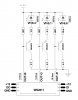
Here is the simulation of the final optimized version. This simulation matches measured values accurately.
https://tinyurl.com/Schematics-WS2811-CCR

Based on real-life measurements the average sinking current of WS2811 is around 16.5ma (not 18.5 as indicated in the datasheet). In an outside circuit with series resistor value of 610 ohms allowing 20ma, voltage drop of WS2811 to ground was measured at 0.62v with Iws=16.5ma.
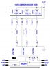
In the main circuit approximate average hfe=Ic/Ib=50, Ie/Ib=49 with Vbe=0.7
Rc=6.2 ohm 2W, Rb=1k 1/4W, Re(r)=9.1 ohm 2W, Re(g)=1 ohm 1/4W, Re(b)=1 ohm 1/4W. The selected resistors are more common resistors which are readily available.
There are a few simple relationships that hold true in this circuit. One can modify resistors as long as certain balance is maintained.
1- Ib=Ie/(1+hfe) (set LED current and then calculate Ib, Ie=I-led)
2- Ic=Ie-Ib
3- Iws=16.5=Irb+Ib (with Ie=300ma, Ib=6ma and Irb=10.5ma)
4- Vrb=Vbe+Vre+Vf (note that this relationship is independent of Vcc, for Vbe at or near saturation =0.7)
5- Vb(min)=0.65
6- For the batch of 10W Common Anode RGB used, average Vf for red, grn, blu were 6.85, 9.3, 9.54 respectively at their individually set I-led (305,293,289).
7- Vce needs to be at or above 0.3v and preferably below 1.4v to keep the transistors from overheating. (TO-92 Package)
8- With Vb-min at 0.65 and Vbe of 0.7 then Ve>=1.35 and Vc>=0.95. To tailor the circuit to your specific currents, decide on individual LED currents for color balancing near 300ma, pick a starting voltage for Vb above 0.65 volts, calculate individual Ib=Ie/50 and Irb=16.5-Ib, set Ve=Vb+0.7, Vc=Ve-0.4, and then calculate resistors (Rb, Rc, Re) based on Vb, Ve, Vc, Irb, Ie, Ic. Side note: With everything biased and fixed, Vce changes with WS2811 current sink (0-16.5ma).
9- Once bias has been achieved Vcc cannot be increased more than 1v or transistors will overheat and will be destroyed for long exposure to this voltage. Vcc can range between 11.8 to 12.6v (Ideal Vcc is about 12.2v). The beauty of this circuit is that it is a constant current and constant voltage. If Vf increases due to overheating, Vrb is increased, Irb is increased and the transistor's Ib is pinched to maintain 16.5ma for Iws. This causes the LED current and voltage to drop, keeping the LED at a constant current. Similarly small drop in Vf causes the reverse effect, increasing LED current to compensate. The circuit will maintain a constant current for Vcc between 11.6 and 13v. For long run of wires between pixels, It is recommended that Vcc is set between 12.2v to 12.6V to avoid noticeable dimming of pixels since voltage drop of 30 feet run of wiring is about 0.6v).
10- LED currents were intentionally selected as such to produce a slightly warmer white with good color mixing for yellow, Magenta, and Aqua-Teal. Power Diss. of Transistors are less than 250mw with no need for any heat-sinks as long as Vce is kept in check (<1.5v).

2N4403: TO-92, Vbe(on)=0.6, Vbe(sat)=0.7, Vce(on)=0.3, Vce(sat)=0.6, Ic(max)=600ma, Pd(max)=625mw

Op-amp, NPN, Voltage reference and Resistor below it represent the constant current sinking of WS2811. With a simple modification this circuit can be used as a dumb constant current driver for high power RGB. Remove WS2811 from the circuit and replace it with a Quad op-amp with a simple voltage divider to produce individual voltage references for the op-amps.

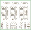
Added resistors to achieve the appropriate bias increases power consumption by only 3.4%. This extra power consumption is mostly compensated by running the LED's at their optimum currents below their maximum ratings, increasing life of LED's. Total circuit current consumption including WS2811 overhead is about 1A per RGB pixel which translates to an approximately 12W in power consumption per pixel. The pcb board is small enough to easily fit inside the metal casing of power LED (1-inch x 2.25-inch). Total part cost including pcb is about $1.50 which meets the original set requirements of this post. The ultimate goal of this project is to utilize a low cost interface to convert a "Dumb" 10W RGB Pixel into an "Intelligent" Pixel while providing the Pixel with a constant current. This allows the user to control a large number of High Power pixels by setting individual brightness and colors, utilizing some of the more common SPI and PC based controllers available on the market.
 
Last edited:
Status
Not open for further replies.

Latest threads

Back
Top