Continue to Site

Welcome to our site!

Electro Tech is an online community (with over 170,000 members) who enjoy talking about and building electronic circuits, projects and gadgets. To participate you need to register. Registration is free. Click here to register now.

  • Welcome to our site! Electro Tech is an online community (with over 170,000 members) who enjoy talking about and building electronic circuits, projects and gadgets. To participate you need to register. Registration is free. Click here to register now.

SMT Prototyping Methods

Galgso

Member
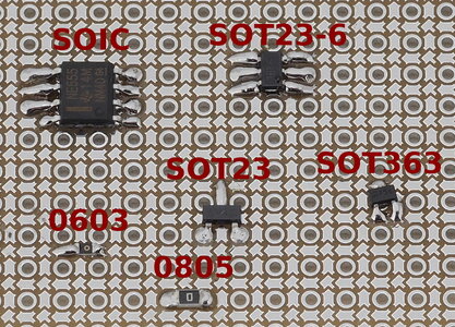
I was looking into different methods for making prototypes with surface-mount components and I stumbled upon this prototyping board design (see attached image). Here's a link to the github page of the person who designed the board in the attached image: https://github.com/electroniceel/protoboard.

I was wondering whether anyone here has any experience with these boards or something similar. I usually do point-to-point prototypes or solder components to a ground plane (copper clad board) but neither of these techniques work very well with surface mount components although I imagine it would not be impossible to use a copper clad board for larger SMT packages (1206, SOT-23, etc.).
 

Attachments

  • packages.jpg
    packages.jpg
    269.1 KB · Views: 8
Breakout boards are available in many footprints, usually broken out to 0.1" headers for use with a breadboard.

Amazon has many variations.

Screenshot_20250724_164926_Edge.jpg
 
Breakout boards are available in many footprints, usually broken out to 0.1" headers for use with a breadboard.

Amazon has many variations.

View attachment 150352
I was aware of the availability of breakout boards but was looking for a prototyping method directly compatible with surface mount components. The board I've linked to should in theory allow one to use both surface mount components and through-hole components on the same board although I've never used one so I'm unsure of the downsides of using such a board. If no-one here has tried the boards I've linked or something similar I'll probably still get some to try and report back because they would be really useful if they work as intended and eliminate the need for breakouts for 1.27mm pitch ICs and 1206s.

I'm a bit averse to using breadboards generally unless I know I'll be replacing components frequently because I get the issue of dodgy connections sometimes unless I really take my time when constructing the circuit. Soldering circuits together makes the likelihood of dodgy connections far smaller which is important when you're scratching your head trying to figure out why your circuit's not working. That's just my experience though It may be a skill issue I don't know.

As a sidenote 1206s and SOT-23 transistors do work with standard 2.54mm pitch matrix boards but SOIC chips don't.
 
It's unclear on that board how the pads are interconnected, if at all. I like interconnections like in the typical solderless breadboards.

I was frustrated with the usual breakout boards (BOB) as they are expensive and take up a lot of space on a solderable breadboard. (I have used solderable breadboards almost exclusively for the past several years.) So, I made a first roll of a version with footprints for common 0.05" SMDs:

1753436766936.png


1) Square pads were tried to facilitate adding two-terminal devices in 805 and 1206 sizes (both are shown placed at the top). The jury is still out on that. They make cutting tracks a little more difficult.
2) I put some common footprints in the center. The SOIC8 routing, if retained, has been redone much better. For the 3- and 6-pad devices, I am not sure both are needed. I may revert on roll#2 to just 6-pad or just 3-pad.
3) I like TH and will probably retain that option on future versions as the smallest (1/8W) fit nicely, and the leads can help avoid adding jumpers, thus saving space.
4) I like the PCB interconnects on only one side (bottom) as it makes it easier to cut interconnections when needed. The cheapest boards from China have the interconnects on both sides. SparkFun's are only on one side.
 
Here's a soldered simple example from last Winter. The central pads were not used as the one I needed was not nearby. That is why I am considering making all the center footprints 6-pin. You can see where leaded resistors were used to jump columns without using jumpers.

1753439090513.png
 
It's unclear on that board how the pads are interconnected, if at all. I like interconnections like in the typical solderless breadboards.
1753453065910.png

1753454166757.png


The pads are not interconnected at all, but there is a ground plane on the bottom layer. The outer circular pad connects to ground and the inner circular pad is just the other side of the plated hole on top. To connect a pad to the ground plane, you can just solder the inner ring to the outer ring on the bottom layer.

I like interconnections like in the typical solderless breadboards.
The board I linked is probably not a very good solution for those who prefer a breadboard-style prototyping board. I prefer matrix boards becasue they allow for more freedom at the expense of having to add more jumpers. I think your board design would can be improved if make the middle area of the board look like the board I posted whilst keeping the rest of the board identical. That way you have compatibility with SOIC packages and SOT-23 transistors while still preserving the breadboard-style interconnections on the rest of the board.
 
Ahhh. That's an interesting way to allow easy ground connections. It does require careful soldering and attention to detail.

On micro boards I've designed, I have provision for pull-up/pull-down resistors for some port pins using 3 pads for a vertical resistor. One leg to the port pin, and the other to either Vcc or ground. Adding a concentric ring to ground on the bottom and Vcc on the top allows the selection to be made without an extra pad.

Hmmm. The same technique could be used for I2C address pins.
 
Adding a concentric ring to ground on the bottom and Vcc on the top allows the selection to be made without an extra pad.
What do you mean? Do you mean splitting the outer circular pad into two isolated arcs? I was thinking about this myself but I imagine that may be difficult to manufacture as the designer said he had trouble getting JLCPCB to fabricate his board and had to use Elecrow.
 
Or maybe something like this on the bottom layer:
1753457375256.png


I would have to think about how the stack-up should look like though because the gnd layer should ideally be right under the signal layer to allow high-speed signals (high frequency, fast rise time or both) to travel in the dielectric space between the signal trace on top and the GND plane. This also raises an interesting question: what would the ideal SMT prototyping board for RF circuits look like?
 
No.... I think that would be a nightmare!

A ring on the bottom layer to ground, as shown in post #6, and a similar ring on the top layer to Vcc. Short the top for pull-up. Short the bottom for pull-down. Short both to let the magic smoke out 😉
 
I created a foot print for a Vcc / ground solder jumper pad.

The upper left picture shows how I have done a selectable pull-up / pull-down resistor arrangement using 3 pads. The square pad with the circle is the resistor connection to the port pin. The other 2 pads are Vcc and ground, with the other end of the resistor connected as desired.

The bottom pictures show both sides of a board with the solder-jumper pad. It's built by putting a top copper and bottom copper ring around the desired size pad. The trick is to duplicate the top and bottom copper rings in the top and bottom soldermask layers. Remember, the soldermask layer is a negative layer - you draw where you don't want soldermask (i.e., where you want exposed copper).

solder jumper pad.jpg
 

Latest threads

New Articles From Microcontroller Tips

Back
Top