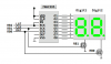
Continue to Site

Welcome to our site!

Electro Tech is an online community (with over 170,000 members) who enjoy talking about and building electronic circuits, projects and gadgets. To participate you need to register. Registration is free. Click here to register now.

  • Welcome to our site! Electro Tech is an online community (with over 170,000 members) who enjoy talking about and building electronic circuits, projects and gadgets. To participate you need to register. Registration is free. Click here to register now.

Serial Data Out from 16f690 to 74HC164

Status
Not open for further replies.
I also don't think you need an additional latch IC but I would still blank the display while loading the shift register.

Angry Badger, you should be able to change the software "segment table" to match the way you wired the segments, or easier still, shift out the serial bits in the reverse order.

Mike
 
Last edited:
A latch is needed if he wants to show a number/alpha on the 7 seg without seeing it being shifted in :)

I rather have a number popup then see it slide in as jumbled stuff.
 
Last edited:
No, it's not necessary. The data you shift in stays on the outputs so all you need to do is;

(1) turn off the old digit common cathode or common anode transistor (blank the display).

(2) load new digit 8 bit segment data into the shift register.

(3) turn on the new digit common cathode or common anode transistor.

Duh!
 
Last edited:
That is 1 one he can do it.

But he can also just use the latch. They both will accomplish the same thing. and require one pin extra.

The point is he has many options.
 
Agreed! There are an almost unlimited number of ways to do it.

Do you know how to do it with 3 pins total using a 74HC595 and two transistors for his 2 digit display?
 
Last edited:
Hi,

I've done away with the latch - I just turn the digit off whilst loading the data.

Code:
;PART OF CODE:	
Main:
    movlw   .7                  ;serial data has to be shifted seven times
    movwf   shift_count     
    movfw   units               ;zero at start-up, incremented later by button
    call    Binaryto7seg        ;get led segment data corresponding to value of 'units'
    movwf   LED1
Shift_bits:
    rrf     LED1
;determine state of data bit  
    btfsc   STATUS,C        ;is the data bit '1'?
    bsf     PORTC,0         ;yes, copy the data bit to the port bit
;data clk        
    bsf     PORTC,1         ;clk pulse low to high shifts data bit into Q0 74HC164
    bcf     PORTC,1         ;clk pulse low
    bcf     PORTC,0         ;set it to '0' if it had been set to '1'
    decfsz  shift_count
    goto    Shift_bits
;turn the digits on/off
    call    Display
;test the switch input    
    btfsc   PORTA,0                 ;is RA0 low (switch pressed)?
    goto    Main                    ;no
;count up    
    incf    units                   ;yes
    movlw   .10
    subwf   units,w
    btfsc   STATUS,Z
    clrf    units
;test the switch input    
    btfsc   PORTA,0                 ;is RA0 high (switch released)?
    goto    Main                    ;yes
    call    Display                 ;no
    goto    $-3                     ;loop until switch released     
 
    goto    Main                    ;no
    
;__________________________________________________________________________________________________________	
   
Display:
;Digit_on_time:
    bsf     PORTC,7         ;Drive the mosfet to show the digit   
    clrf    TMR2
    btfss   T2_done
    goto    $-1
    bcf     T2_done  
;Digit_off_time:    
    bcf     PORTC,7
    clrf    TMR2
    btfss   T2_done
    goto    $-1
    bcf     T2_done
             
    return
 
would it require 1 npn and 1 pnp?

No, I'll draw a sketch and attach it in a little while. It's really simple.

Here's the sketch...

brain-teaser-png.29729


When we're displaying digit 1 or digit 2 the RB2 pin is low which enables the '595 outputs and the RB0 and RB1 pins are setup to enable one of the column driver transistors.

When we're updating or refreshing the display we set the RB2 pin high which disables the '595 outputs and blanks the display. This also takes the RCK (latch) pin high so data clocked into the shift register goes immediately onto the output latches but this doesn't matter because the outputs are turned off so we won't see anything funny on our display. Now we retask our RB0 ad RB1 pins for use as SER (DAT) and SCK (CLK) lines to load the '595 shift register. While we're using RB0 and RB1 to load the shift register we're also inadvertently turning the column driver transistors on and off but this doesn't cause a problem because, again, the '595 segment driver outputs are off (the display is off).

Here's an untested ISR driver example;

Code:
;
;  three pin two digit display
;
;  unsigned char digit1 = 0;    // 0..9
;  unsigned char digit2 = 0;    // 0..9
;  unsigned char column = 1;    // 00000001 or 00000010
;
;  #define DAT portb.0          // DAT and digit 1 select pin
;  #define CLK portb.1          // CLK and digit 2 select pin
;  #define LAT portb.2          // shift register LAT & OE pins
;
;  void isr_display()
;  { unsigned char work;        //
;    unsigned char i;           //
;    pir1.TMR2IF = 0            // clear timer 2 interrupt flag
;    if(column.0 == 0)          // if last digit was digit 2
;      work = segtbl[digit1];   // get segment data for digit 1
;    else                       // else
;      work = segtbl[digit2];   // get segment data for digit 2
;    LAT = 1;                   // LAT/OE = 1, blank the display
;    for(i = 0; i < 8; i++)     // load the shift register
;    { CLK = 0; DAT = 0;        //
;      if(work.0) DAT = 1;      //
;      CLK = 1;                 // clock bit into SR
;      work >>= 1;              //
;    }                          //
;    column ^= 0b00000011;      // flip digit select bits
;    portb = portb & 0xF8 | column;  // turn on display
;  }                            //
;
There are a few subtleties to the code. It's important to leave the SCK (CLK) pin high after loading the shift register so that when we set RB0 and RB1 to enable the column drivers we'll never get a low-to-high transition on the SCK pin and clock in an unwanted bit. Also, we set the RCK and EN pins back to '0' to turn on the display in that very last instruction when we AND port B with 0xF8.

Anyway, sorry to detract from the original posters thread.

Regards, Mike
 

Attachments

  • Brain Teaser.PNG
    Brain Teaser.PNG
    19 KB · Views: 3,914
Last edited:
I think i get it lol

So you send data as normal when latch isnt on then latch it and set either the RB1 and RB0 depending on digit. then repeat by sending the appropriate data then latching?

EDIT:
I must ask sorry to go off topic but what program are you doing that nice drawing in?
 
Last edited:
Yes Jason, I think you've got it. Basically we use RB0 and RB1 as column driver lines during display "on" time and retask them for use as DAT and CLK signal lines during display "off" time to load the shift register.

One really neat thing about this method is that you can use a PWM signal on the RCK + EN pins for complete fade-to-black brightness control.

Regards, Mike
 
serious? Dude how? info info :D i have Office 2007 somewhere on dvd here. I gota reinstall that sucka lol

Im learning autocad inventor right now :D its nice!
 
Jason, you can't be serious. I just saw some sketches you posted the other day that blew my socks off. They were really heavy duty man (LOL)...
 
Last edited:
im learning the 3d stuff for fun but the Autocad Inventor i want to learn so i can make custom parts like:

Plastic Cases, Connectors and stuff. Like if i was to make something then find out i can make money from it and then have to learn this stuff it would suck because byt the time i learn it its too late :D so i learn now and be prepared for later :D even if it doesnt come then i still gained experience.

EDIT:
Thanks! But i like the way those schematics come out. So life like and makes me want to do it lol
Do you have more info on how you do it?
 
Last edited:
Hi,

I've done away with the latch - I just turn the digit off whilst loading the data.

Code:
;PART OF CODE:    
Main:
    movlw   .7                  ;serial data has to be shifted seven times
    movwf   shift_count     
    movfw   units               ;zero at start-up, incremented later by button
    call    Binaryto7seg        ;get led segment data corresponding to value of 'units'
    movwf   LED1
Shift_bits:
    rrf     LED1
;determine state of data bit  
    btfsc   STATUS,C        ;is the data bit '1'?
    bsf     PORTC,0         ;yes, copy the data bit to the port bit
;data clk        
    bsf     PORTC,1         ;clk pulse low to high shifts data bit into Q0 74HC164
    bcf     PORTC,1         ;clk pulse low
    bcf     PORTC,0         ;set it to '0' if it had been set to '1'
    decfsz  shift_count
    goto    Shift_bits
;turn the digits on/off
    call    Display
;test the switch input    
    btfsc   PORTA,0                 ;is RA0 low (switch pressed)?
    goto    Main                    ;no
;count up    
    incf    units                   ;yes
    movlw   .10
    subwf   units,w
    btfsc   STATUS,Z
    clrf    units
;test the switch input    
    btfsc   PORTA,0                 ;is RA0 high (switch released)?
    goto    Main                    ;yes
    call    Display                 ;no
    goto    $-3                     ;loop until switch released     
 
    goto    Main                    ;no
    
;__________________________________________________________________________________________________________    
   
Display:
;Digit_on_time:
    bsf     PORTC,7         ;Drive the mosfet to show the digit   
    clrf    TMR2
    btfss   T2_done
    goto    $-1
    bcf     T2_done  
;Digit_off_time:    
    bcf     PORTC,7
    clrf    TMR2
    btfss   T2_done
    goto    $-1
    bcf     T2_done
             
    return

Hi Angry Badger,

So CLK = portc.1, DAT = portc.0, and digit1 = portc.7, right? What about digit2? Is it connected to a port pin?

How are you developing your delays?

Mike
 
Last edited:
By the way Atomsoft, don't install 2 year old software. Download Openoffice if you need to open MS stuff.
 
Hi Angry Badger,

So CLK = portc.1, DAT = portc.0, and digit1 = portc.7, right? What about digit2? Is it connected to a port pin?

How are you developing your delays?

Mike

Hello Mike,

Haven't got around to the other digits yet! I'm now in the middle of my 4 x 12 hours work shift pattern so no time for PICs! Will attack the other digits next week.
 
Status
Not open for further replies.

Latest threads

New Articles From Microcontroller Tips

Back
Top