Continue to Site

Welcome to our site!

Electro Tech is an online community (with over 170,000 members) who enjoy talking about and building electronic circuits, projects and gadgets. To participate you need to register. Registration is free. Click here to register now.

  • Welcome to our site! Electro Tech is an online community (with over 170,000 members) who enjoy talking about and building electronic circuits, projects and gadgets. To participate you need to register. Registration is free. Click here to register now.

Separate Brake Light From Turn Signal

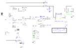
Two things. Firstly, do not connect the outputs of U2c or U2d to anything. Unused inputs on CMOS ICs are bad, but unused outputs don't matter. Connecting them as you have will lead to more power dissipation.

Secondly, I suggest that you have the power supply to U1 and U2 separate from the power supply to M1. Either fit two more diodes from the two inputs to feed U1 and U2, or have a diode from the supply to M1 and feed the U1 and U2 from that diode. Have another capacitor for U1 and U2. That way the supply for U1 and U2 will continue if the supply for M1 drops when both lights are off.

A final suggestion would be to feed the logic inputs, U1a, U1c, R4 and R5 via diodes from the inputs. Without that the circuit will fail instantly if the polarity is wrong.
run-1.png

Please let me know what I have missed.
 
Last edited:
HI

All of the inputs of unused gates (U2C, U2D) should be connected to either +V or ground. Outputs should be left unconnected. If the gate inputs are not connected, spurious oscillation can occur and cause needless power dissipation.
 
I suggest that you have the power supply to U1 and U2 separate from the power supply to M1.
Not needed.
No problem if the supply voltage drops to zero when the tail lights are not lit.
Why do you think there would be?
feed the logic inputs, U1a, U1c, R4 and R5 via diodes from the inputs. Without that the circuit will fail instantly if the polarity is wrong
Again, not needed.
How could the polarity be "wrong"?
 
Please let me know what I have missed.
D5 and D7 will not work since there is no path for the input to go to zero (open is not zero).
Remove them.
D6 is redundant.
Also remove

But for added input protection, you can add a 10kΩ resistor is series with each set of inputs.
(Below):

1716426330005.png
 
But for added input protection, you can add a 10kΩ resistor is series with each set of inputs.
(Below):
OK, I have made the changes. I got just one Vdd question. You show Vdd at C3. So I supplied power to the 4039's on that "net" Design Spark calls them nets. (The "green" net is VDD)
run-1.png
 

Attachments

  • run-1.png
    run-1.png
    21.8 KB · Views: 37
Last edited:
You show Vdd at C3. So I supplied power to the 4039's on that "net" Design Spark calls them nets. (The "green" net is VDD)
Yes, Vdd is a net name.
 
There is no ground terminal on the PCB?? If the rest of the connections are by terminals, I'd suggest one for ground as well - that allows you to test the circuit it with more accessible, hanging on wires, rather than bolted to something.

I'd suggest adding a 100 Ohm resistor and 15V zener between the FET source feed and the 4093 power, just to protect from electrical spikes.

Another thought; if you rotated the FET package 90' clockwise, you could take the V+ track to the right & though the centre of U2, with the link between 7 & 8 of that using vias to the ground plane. That would eliminate the vias in the high current path through the FET. The IC grounds are far lower current.

ps. Check the FET part number & pinout? The schematic shows a dual FET package?
 
I'd suggest adding a 100 Ohm resistor and 15V zener between the FET source feed and the 4093 power, just to protect from electrical spikes.
OK, ill add and post changes
Another thought; if you rotated the FET package 90' clockwise, you could take the V+ track to the right & though the centre of U2, with the link between 7 & 8 of that using vias to the ground plane. That would eliminate the vias in the high current path through the FET. The IC grounds are far lower current.
I'll give it a whirl. Thank you
 
You should put resistors in series with with both inputs of U1D.

At the moment that the brakes turn off, both C1 and C2 will be charged. The supply voltage on C3 will be pulled down by the brake light, then the input clamping diodes in U1, which stop the inputs getting more than 0.6 V above the supply, will start to conduct.

It's very difficult to know exactly how much current will flow in the clamping diodes. Obviously when the inputs turn off, the MOSFET should turn off. Once that has happened, there will be nowhere for the current to flow from C3. However the MOSFET will take some time to turn off because of R1, so it's a bit of a race so there could be little current, or it could get to quite a high level before the MOSFET turns off.

If you do get current flowing from C1 and C2, via the MOSFET to the brake lamp, then the current in the clamping diodes could be near the brake light current, and that would be far more than you should be putting through the input clamping diodes. That current will be happening every time you release the brakes, or at the end of every flash if the hazard lights are on.

If you add 10 kOhms in series with each input, the current is limited to about 1 mA and it can't do any harm.
 
You should put resistors in series with with both inputs of U1D.

At the moment that the brakes turn off, both C1 and C2 will be charged. The supply voltage on C3 will be pulled down by the brake light, then the input clamping diodes in U1, which stop the inputs getting more than 0.6 V above the supply, will start to conduct.
If you could just use my schematic and place a mark so I know where to put the 10k resistors I'd be grateful. RJ suggested a zener and resistor but I need clarification.
 
Again, not needed.
How could the polarity be "wrong"?
It's really easy to wire things up wrong. It's standard practice in automotive work to protect stuff against reversed polarity, and most appliances like routers have diode on the input even though they are supplied with a power supply and a plug that can't be put in the wrong way round.

I recently posted this:- https://www.electro-tech-online.com...rear-windows-to-passenger-side-of-car.165710/
The circuit diagram is based on the typical circuit in the data sheet of the NCV7471B system basis chip, and that has a diode on the input as it is a standard precaution.
 
It's standard practice in automotive work to protect stuff against reversed polarity,
Okay, but my circuit is protected by the added input resistors and diodes already there.
 
It's really easy to wire things up wrong. It's standard practice in automotive work to protect stuff against reversed polarity, and most appliances like routers have diode on the input even though they are supplied with a power supply and a plug that can't be put in the wrong way round.
I appreciate the added protection. I've added the resistors and re-worked the vias so they are closer to the pads. I think I read somewhere that was good practice. Also Added GND copper pour to bottom layer and a small pad to the ground screw.
PCB01.png
 
You might want test points. I suggest the logic gate outputs and the power supply.

I would also add space for a ceramic capacitor between +ve and ground at each IC. I very much doubt it would be needed on a circuit that runs as slowly as this and that has such large voltage tolerances, but it can't hurt and you have loads of space.
 
You might want test points. I suggest the logic gate outputs and the power supply.
OK Design Spark not good at making test points so I added top layer pads and included a legend with reference points to the relevant pads.
I am going to order the mosfet and the 2 resistor values I need in a few days. Member rjenkinsgb had a concern about the mosfet I selected. let me know if I got it wrong.

PCB01.png
 
Back
Top