ThomsCircuit
Well-Known Member
I'm glad I got the pot's wired correctly.
I was able to increase the trace that requires 3 amps to 70

I was able to increase the trace that requires 3 amps to 70
Follow along with the video below to see how to install our site as a web app on your home screen.
Note: This feature may not be available in some browsers.

SCHEMATIC. Detail Mosfet IRF5305
The mosfet gate can be a narrow trace. The mosfet drain and source need to be a fat trace.I'm glad I got the pot's wired correctly.
I was able to increase the trace that requires 3 amps to 70
View attachment 145999
OK got it. I did think that was not right but the images were throwing me off.The mosfet gate can be a narrow trace. The mosfet drain and source need to be a fat trace.
The other side of D8 needs to be fat to the V+ pin.
OK got it. I did think that was not right but the images were throwing me off.
So what I did now was
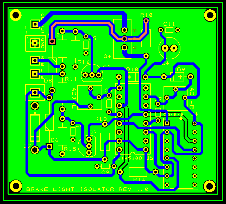
gate: trace is narrow (30)
Source: I moved that trace to the bottom layer and added a rectangular pour
Drain: Left that trace on the top layer and added a custom shape pour.
I also added a small rectangular pour on the other side of D8 where it connects to the positive input also on the bottom layer.
View attachment 146000
Made the changes. Moved the mosfet so it can be laid down with heat sink facing up. Larger spokes on the small VDD pour and removed the other pours. Altered components so they can be identified from the bottom.1. I think the fat Source and Drain traces without the pours will be fine.
2. VDD pour: make the thermal pad(s) spokes fatter without violating rules.
I think you can do this in DSPCB by pointing at each spoke and setting the width.
I am making both. Its only a few dollars and you were so kind to assist me. I will have a bit of down time for about a month as I am having bi-lateral knee replacement in a few days so while I cannot install the new lights on my trailer I can sit and solder. I have located all the components and am just fine tuning the layout. On another note I have learned a great deal as I can make decisions on alternate parts, make & read schematics, layout components for PCB fabrication and understand suggestions from members and make corrections.As you still considering also building the circuit I proposed, or are you just going with this one?
Made the changes. Moved the mosfet so it can be laid down with heat sink facing up. Larger spokes on the small VDD pour and removed the other pours. Altered components so they can be identified from the bottom.
View attachment 146023
No, but I had a Subway meatball sub a few days ago.By the way did you get yourself a plate of meatballs?
I took care of it. Relocated the Out+.Don't change anything, but it would make more sense if the mosfet was moved next to the OUT+ terminal
Thermal pads are only needed for pins that connect to a pour. Thermal pads are intended to act as a "thermal isolators" so that the pin can be heated enough to be soldered. If there is no pin, and a thru hole connection is needed, then the hole should be an ordinary via.These are ground vias. A ground bottom layer copper pour added the spokes. I don't need these do I? Design Spark allows me to change their isolation so they wont have any. Should I?
Thought so. Thanks.If there is no pin, and a thru hole connection is needed, then the hole should be an ordinary via.
Actually, they are to provide some thermal isolation, so the ground copper ground plane doesn't conduct so much heat away, that it's hard to solder the pin.Thermal pads are intended to act as a "thermal conductor" so that the pin can be heated enough to be soldered.
Yes. Agreed. That's what I meant. It's actually a "thermal isolator".Actually, they are to provide some thermal isolation, so the ground copper ground plane doesn't conduct so much heat away, that it's hard to solder the pin.
I used a site to help me get a equal on/off time in a period of .8 seconds. Similar to my trucks cycle. I can replace R2 (24k) with a 50kpot to adjust.
Interesting. Well, without getting to complex is that an issue with this circuit? Would that prevent me from synchronizing the trailer circuit?the NE555 won't get 50/50 duty without special circuitry.
You mean at pin 3 of the 555 output? If so perhaps adding a transistor to increase the output so it can drive the trailer circuit. If that's the concern.the drive output is very limited (max 50ma@15v)

