Continue to Site

Welcome to our site!

Electro Tech is an online community (with over 170,000 members) who enjoy talking about and building electronic circuits, projects and gadgets. To participate you need to register. Registration is free. Click here to register now.

  • Welcome to our site! Electro Tech is an online community (with over 170,000 members) who enjoy talking about and building electronic circuits, projects and gadgets. To participate you need to register. Registration is free. Click here to register now.

Separate Brake Light From Turn Signal

This is a component/logic driven option. Difficult to make out what the components are though. Site says free for private use.
3rd_light_circuit.gif
 
Last edited:
It's not clear to me that any of the other circuits posted here operate properly for the combined signals of one side blinking and the other side steady-on, indicating a combined turn and braking situation.
Below is the LTspice sim of one that does:
It uses two CD4093 Schmidt-trigger NAND gate ICs.
The basic logic is:
  • U2 is configured as a latch that controls the center brake light
  • When both the turn signals (blue and green traces) are high at the same time, this indicates a braking condition and the latch is set, energizing the brake light (green trace)
  • When both signals go low, indicating no signal or just a blinking turn, the latch is reset and the brake light goes off
The diodes, resistors, and capacitors at the input to U1d, are to provide a short-term memory of the turn-signal blinking, to avoid the possible delay otherwise of up to 1/2 the blink period before the brake light comes on (which is obviously not desirable).

(The circuit generating the combined signals is not shown, so only the circuit needed to generate the brake light function from the left and right turn-signals is visible.)

1716361608203.png
 
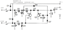
The circuit diagram is made a lot less clear by having
1716358961211.png
to show four wires joining and having
1716359000959.png
to show two wires crossing without joining.

This is my slight re-draw that never has four wires joining at a point, and has more visible dots at the joins.

1716362090144.png


It also has component numbers that are visible and I have called the final output transistor Q3

The circuit gives the same overall behaviour as the relay circuit, but it switches the negative of the centre brake light, not the positive. The centre brake light is connected on the right between LED+ and LED-

When only left is turned on, the current will flow through R1 and R3 to the emitter or Q1. Some of that current will flow through R4 and R5, so Q1 will turn on and the voltage at the emitter of Q1 will remain low. Q2 will be turned on by R6 so Q6 will keep the voltage low at the gate of Q3 and Q3 will be off.

When only right is turned on, Q1 and Q2 remain off. D4 keeps the voltage on it low, so that the base-emitter breakdown voltage of Q1 and Q2 is not exceeded. The emitters of Q1 and Q2 remain at low voltages, and Q3 will be off.

When both left and right are on, D4 and D5 keep the voltages the same on the base and emitter of Q1, so it stays turned off and current can flow through R3 and D5 to turn on Q3 and the brake light comes on.

If left then turns off, with right remaining on, the base voltage of Q2 is kept high from the right signal, via R5 and D7, so C1 remains charged and Q3 stays on.

If right turns off with left remaining on, the base voltage of Q2 is kept high from the left signal, via R1 and D6, so C1 remains charged and Q3 stays on.

When both left and right turn off, the base of Q3 is pulled down by R6 and then C1 is discharged ready for the next operation.

In summary, when both left and right are on, C1 is charged, When both left and right are off, C1 is discharged. If only one of left and right is on, C1 is remains in its previous state. When C1 is charged and either light is on, the brake light will be on.

So I think that the circuit works fine. However, some components need choosing carefully. Q1 and Q2 have their base-emitter junctions reverse-biased by a voltage equal to the zener voltage of D4 and D5. If there is any leakage through Q1 or Q2, that will charge C1. That condition should only go on for a short time, so some leakage won't hurt, but it's not something I am completely happy about.

Also, when left only is on, the circuit relies on Q1 keeping the voltage on its emitter very low, and if the voltage on right doesn't stay very low, then you could get some voltage charging C1
 

Attachments

  • 1716361248749.png
    1716361248749.png
    27 KB · Views: 32
The basic logic is:
  • U2 is configured as a latch that controls the center brake light
  • When both the turn signals (blue and green traces) are high at the same time, this indicates a braking condition and the latch is set, energizing the brake light (green trace)
  • When both signals go low, indicating no signal or just a blinking turn, the latch is reset and the brake light goes off
I agree with the logic. However there is no need for the large RC delays on U1d. I don't think that there is a need for any delay.
 
It's not clear to me that any of the other circuits posted here operate properly for the combined signals of one side blinking and the other side steady-on, indicating a combined turn and braking situation.
Below is the LTspice sim of one that does:
It uses two CD4093 Schmidt-trigger NAND gate ICs.
You and Diver300 are an amazing pair of individuals. Taking the time to help me solve my issues is incredibly generous of you. I do appreciate you and thank you for helping me.
 
The circuit gives the same overall behaviour as the relay circuit, but it switches the negative of the centre brake light, not the positive. The centre brake light is connected on the right between LED+ and LED-
Considering how old and blurry this circuit is and you were able to bring it into focus is pretty incredible.
If there is any leakage through Q1 or Q2, that will charge C1. That condition should only go on for a short time, so some leakage won't hurt, but it's not something I am completely happy about.
knowing how some knock off components are made these days it may be difficult to obtain ICs that are reliable. At least as a hobbyist it would be as I have been known to shop at such places.
 
So I think that the circuit works fine.
However there is no need for the large RC delays on U1d. I don't think that there is a need for any delay.
You are both not considering one critical sequence.

What about when one side is already blinking and the other side then turns on for the brake when the blink is low?
The memory (not delay) from the Diode-R-C circuit in my design remembers (for a short period) that the one side is blinking, so the brake light can turn on instantly, not having to wait until the blink side goes high again.

Waiting for the blinking side to go high (typically up to a half second) before the brake light comes on is an unacceptable delay for a brake light, and I think all the other suggested circuits have that possible delay.

Am I wrong?
 
Waiting for the blinking side to go high (typically up to a half second) before the brake light comes on is an unacceptable delay for a brake light
I myself prefer the instant option.
I am looking at the IRF7406 and it is an 8 pin surface mount but your schematic shows just 3 connection points. I understand the mosfet is a P channel and I could use different one with the following requirements...

Drain to Source Voltage 30
Drive Voltage 4.5-10
Vgs 1V @ 250µA
 
I am looking at the IRF7406 and it is an 8 pin surface mount but your schematic shows just 3 connection points.
That should work fine.
The package has 8-pins, but the source and drain have parallel pin connections to give the the 3 transistor connections:
1716389242699.png
 
That should work fine.
The package has 8-pins, but the source and drain have parallel pin connections to give the the 3 transistor connections:
I see that pins 5-8 are joined so I could use one or tie all 4 together. The same with pins 1,2, and 3
 
7406.png

I would connect it in the schematic like this. DesignSpark 11
And I notice your circuit requires a constant power source. Vdd. Sot this circuit would work with 5 and 7 wire hookups as 4 pin does not have one.
 
Last edited:
You are both not considering one critical sequence.

What about when one side is already blinking and the other side then turns on for the brake when the blink is low?
The memory (not delay) from the Diode-R-C circuit in my design remembers (for a short period) that the one side is blinking, so the brake light can turn on instantly, not having to wait until the blink side goes high again.

Waiting for the blinking side to go high (typically up to a half second) before the brake light comes on is an unacceptable delay for a brake light, and I think all the other suggested circuits have that possible delay.

Am I wrong?
I agree, the delay would help in that case.
 
And I notice your circuit requires a constant power source. Vdd. Sot this circuit would work with 5 and 7 wire hookups as 4 pin does not have one.
You could supply the logic-gate circuit with two diodes, in the same way that the relay circuit does. When both inputs are low, the light turns off anyhow so you don't need power.

I would suggest a large capacitor to run the logic gates, and a seperate diode to stop that being discharged by the stop light if the stop light was on for a moment without power. That way the capacitor would keep the logic running when no lights were on.

With the delay circuits that crutschow mentioned and explained the reason for, it would be good to keep the electronics running for a lot longer than the delay times.
 
You could supply the logic-gate circuit with two diodes, in the same way that the relay circuit does. When both inputs are low, the light turns off anyhow so you don't need power.
It certainly is not a problem for me but when I re-create the schematic in my program I will add the 2 diodes, we'll see how I do.
I would suggest a large capacitor to run the logic gates, and a seperate diode to stop that being discharged by the stop light if the stop light was on for a moment without power. That way the capacitor would keep the logic running when no lights were on.
While I can easily increase a capacitor from 10 - say 20 or higher I would not know exactly where to place the diode. Ill post a schematic then we can adjust it.
As it is I have all but the 7406 in and one of the resistors in SMD.
 
Here is my first schematic. Once I have this correct we can increase the capacitor and cancel the need for the constant power @ M1
run-1.png
 
Here's the circuit powered from the turn-signal lights:
(The delay circuit causes an occasional extra brake pulse when the braking ends, such as at the 14s time in the sim, but that shouldn't be a problem to those following the vehicle.)

Do you know how much current the brake light takes?
That will determine the required current rating of the diodes.
(The diodes shown are 3A).

1716402143569.png
 
Last edited:
Updated schematic with additional diodes and capacitor.
Need to know how to power the 4093's
EDIT. I found a few mistakes. RTB and LTB were not corrected correctly.
run-1.png
 

Attachments

  • run-1.png
    run-1.png
    20.4 KB · Views: 31
Last edited:
Two things. Firstly, do not connect the outputs of U2c or U2d to anything. Unused inputs on CMOS ICs are bad, but unused outputs don't matter. Connecting them as you have will lead to more power dissipation.

Secondly, I suggest that you have the power supply to U1 and U2 separate from the power supply to M1. Either fit two more diodes from the two inputs to feed U1 and U2, or have a diode from the supply to M1 and feed the U1 and U2 from that diode. Have another capacitor for U1 and U2. That way the supply for U1 and U2 will continue if the supply for M1 drops when both lights are off.

A final suggestion would be to feed the logic inputs, U1a, U1c, R4 and R5 via diodes from the inputs. Without that the circuit will fail instantly if the polarity is wrong.
 
Back
Top