Continue to Site

Welcome to our site!

Electro Tech is an online community (with over 170,000 members) who enjoy talking about and building electronic circuits, projects and gadgets. To participate you need to register. Registration is free. Click here to register now.

  • Welcome to our site! Electro Tech is an online community (with over 170,000 members) who enjoy talking about and building electronic circuits, projects and gadgets. To participate you need to register. Registration is free. Click here to register now.

Schmitt trigger NAND gates

Status
Not open for further replies.

BigAdv

New Member
Trouble getting a CD4093B to do what I want.

I am having a bit of trouble using the schmitt triggered nand gates. I maybe (read am) using them incorrectly, thus not getting my expected result.

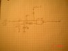
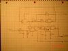
I have gates C and D configured to create an astable multivibrator, and this part works fine, this is to drive a light bulb at 100hrz/50% duty cycle. (6.0v) The output for this is pin 11.

I am using this output (pin 11) as the input to gate A, pins 1. And to gate B pin 5.

Each gate is to drive a separate driver circuit.

There is a separate input signal, that when hi (12v) I would like to turn the output from either gate A or B low. I would also like it to stay low for 340ms after the signal is removed.

So I have pin 2 on gate A and pin 6 on gate B sinked low through a 1M resistor and a cap parallel to the res. And a 10K pull up resistor for the input signal.

The expected results: pin 2 low + pin 1 hi (pwm 6v)= pwm 6v out
Pin 2 hi + pin 1 hi ( pwm 6v)= low (no) out

The actual results: pin 2 low + pin 1 hi (pwm6v)=12v out
Pin 2 hi + pin 1 hi (pwm6v)=pwm 6v out


As you can see, the results are not what I expected. So my questions to the collective wisdom are;

Why am I getting theses results?
Can I make this work?
How can I make this work?
Or do I need a different circuit?

Thank you for any input on this,

Earl
 

Attachments

  • circuit diagram 001.jpg
    circuit diagram 001.jpg
    564.6 KB · Views: 1,106
Do both driver outputs have to be in phase? ie: could the two driver outputs (pins 3&4) come from 2 different oscillators?
 
I would like to keep it all on one ic if possible for the sake of realistate. pcb space is very limited, this part as well as the output driver circuit on a 1"* 2" board. I made a similar system using 555 timers but I thought this would be nice and compact and few components. What did you have in mind?
 
BigAdv said:
I would like to keep it all on one ic if possible for the sake of realistate. pcb space is very limited, this part as well as the output driver circuit on a 1"* 2" board. I made a similar system using 555 timers but I thought this would be nice and compact and few components. What did you have in mind?
hi Earl,
The problem is, even though pin A2 is high when the 12V signal is applied, pin A1 is still connected to the Astable output. [which is going hi/lo]

As pin A1 is set high and low by the astable output from pin A11, being a NAND gate, the 4093 output pin A3 will not stay low....
It will only be low while A1 and A2 are both high.

Truth Table for a NAND.
A2...A1....Output
0.....0........1
0.....1........1
1.....0........1
1.....1........0

Hope this helps.:)
 
hi Earl,
Have a look at this circuit, it works OK.
 
Last edited:
ericgibbs said:
hi Earl,
The problem is, even though pin A2 is high when the 12V signal is applied, pin A1 is still connected to the Astable output. [which is going hi/lo]

As pin A1 is set high and low by the astable output from pin A11, being a NAND gate, the 4093 output pin A3 will not stay low....
It will only be low while A1 and A2 are both high.

Truth Table for a NAND.
A2...A1....Output
0.....0........1
0.....1........1
1.....0........1
1.....1........0

Hope this helps.:)


Eric;

Thank you very much for your replies, this problem keep me up all night. Just could not stop thinking about what was going on. I came to this same concussion, finally went to sleep with the intent to test some more theories tonight. Then I read your post and it all makes perfect sense! So the way I had it set up, if I put a scope on the out put of pin 3 or 4 (with pin 2 low) it should be switching 0 to 12v at 100hz, correct?

I also thought of an other way that I could make this work the way I want it to.

What if I put pin 2 hi through a pull up resistor, and take pin 1 high with the trigger signal?

I tested this and it seems to work the way I what it to, but I am unsure if this is a robust design? Also not sure on the timing circuit to keep it (pin 1) hi? I need the cap to charge fast and then start discharging when the sig is removed. Is this the way to do this? And to calculate the values for the time required is the formula the same? Will all this work as a stable and sound circuit design?

Thank you for the work you did on the circuit for me, this looks good. Is it your own design and if so can I use it if mine does not work out? One question, the diode that you have between pins 11 and 8/9, is this supposed to be a zener? If not don’t get how this works. (Then again I don’t get how a lot of this stuff works!)

This is a diag of the revised circuit that I came up with, any comments or suggestions would be good.

Thanks

Earl
 

Attachments

  • circuit diagram2.jpg
    circuit diagram2.jpg
    521.4 KB · Views: 578
hi Earl,
Could not get on the forum yesterday??

Your version looks OK, you can link pins 1 and 2 and drop the resistor upto +V.
Keep the R and R4 resistors a high value as possible and the C2 as low value as possible.
If the they are too low in value they could pull the output down from the pulse gen, [via the diode] and pins 1/2 on the 4093 would see a sufficient voltage swing.
 
Thanks for the input on this problem. I am used to working in analog type circuits, where what you see with the dvom is what you got, now this is digital, and not so strait forward. The thing that was messing me up was thinking that the 6v pwm signal was just that, 6v. Ofcourse its not, its 12v/0v, so of course it did not work! Now that I got my brain around that, I just might be dangerious!:D

One other question that I have is, at what point does the gate change state? That is what voltage is low and hi, is it 0v and 12v or some other value? Triing to calculate the values for the timing circuit and need to know at what voltage the gate will switch. Also should I use a electolitic cap for the timing or will a ceranic? one work.

Thanks again,
Earl
 
BigAdv said:
Thanks for the input on this problem. I am used to working in analog type circuits, where what you see with the dvom is what you got, now this is digital, and not so strait forward. The thing that was messing me up was thinking that the 6v pwm signal was just that, 6v. Ofcourse its not, its 12v/0v, so of course it did not work! Now that I got my brain around that, I just might be dangerious!:D

One other question that I have is, at what point does the gate change state? That is what voltage is low and hi, is it 0v and 12v or some other value? Triing to calculate the values for the timing circuit and need to know at what voltage the gate will switch. Also should I use a electolitic cap for the timing or will a ceranic? one work.

Thanks again,
Earl

hi Earl,
The switch over voltages [ Vhigh and Vlow thresholds are a function of the supply voltage].
I would download the datasheet for thr HEF4093 from www.datasheetarchive.com
This will give the Vthreshold for some of the common line voltages, the timing resistor/capacitors are close to t= RC
eg: a 1M0 and a 1uF is about 1sec.
The 4093 ic has schmitt inputs, this means the Vth On/Off threshold has 'hysteresis', so if the input signal has a slow rise/fall time,
the output of the 4093 gate will not oscillate at the input voltage threshold.

Depending how critical the timing accuracy is, would for me determine the type of capacitor.
Tantalums are IMO more stable than electrolytic,, a electrolytic would get the job done for your application.

Remember that digital logic, like analog, requires good voltage line decoupling.
A 0.1uF and a 10uf or 47uF would be OK.
 
Last edited:
Status
Not open for further replies.

Latest threads

Back
Top