Continue to Site

Welcome to our site!

Electro Tech is an online community (with over 170,000 members) who enjoy talking about and building electronic circuits, projects and gadgets. To participate you need to register. Registration is free. Click here to register now.

  • Welcome to our site! Electro Tech is an online community (with over 170,000 members) who enjoy talking about and building electronic circuits, projects and gadgets. To participate you need to register. Registration is free. Click here to register now.

Reverse Engineering Hall Affect Sensor For CNC

Status
Not open for further replies.

madaxe

New Member
I have a broken sensor and the original manufacturer has stopped producing. I have no electronics experience, and I'm trying to reverse engineer this thing can somebody help calculate the resistor and capacitor sizes.

i picked these for the bi color led and hall affect sensor

i appreciate any help

Madaxe
uk.rs-online.commin (Volt)max (Volt)forward voltage (Volt)length (mm)width (mm)height (mm)
A1126LLHLT-T Allegro Microsystems, Omnipolar Hall Effect Sensor, 3-Pin SOT-23
3​
24​
3​
2​
1​
2.5 V Green & Red LED 2012 (0805) SMD, Kingbright KPHBM-2012SURKCGKC
2.4​
2​
1.5​
0.5​

BoardLayout.png
 
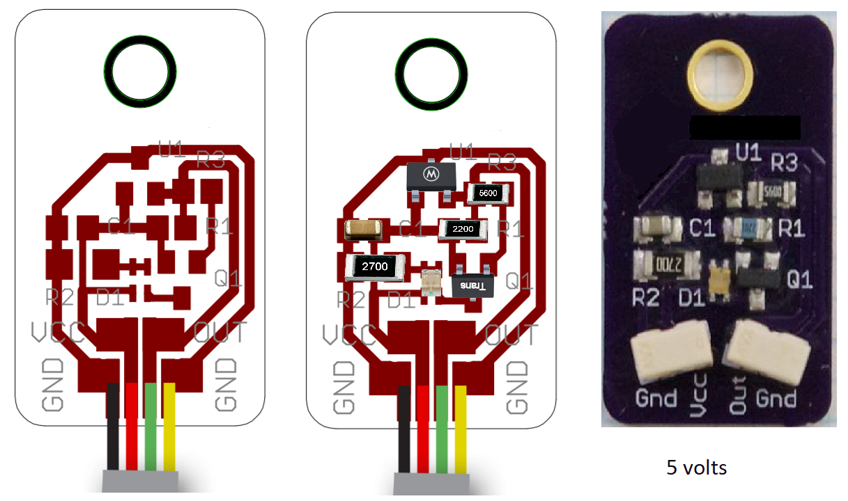
The resistor values are written on them. The first 3 digits are the value, followed by the number of zeros after that value. In this case the last digits are all 0, so there are no more zeros to add, and the values are 270 Ohm, 220 Ohm and 560 Ohm

There is no scale in your photos, but guessing from the Hall sensor size, the 270 Ohms is a 1206 size (0.12 inches long, or near 3mm) and the others are 0805 size (0.08 inches long or near 2mm)

The transistor could be just about any cheap PNP transistor in a SOT23 package. A BC858 is one that I know should work if I've got the size correct.

The capacitor is to smooth the supply. There is no correct value. I guess they would have used 100 nF as that is suggested in the Allegro data sheet. You might be able to unsolder one and measure it.

If you don't need the LED, you can miss it out, along with the transistor, the 270 Ohm and the 560 Ohm resistor. The circuit will operate fine without them if you don't need a visual indication.
 
Thanks for your help, do you know of any good videos on making a BCP, or a website where i can order from, i have a soldering station with heat gun i think i can solder the components to the board. WIll i need a mask?
 
If you want to DIY a circuit board, use Vero strip board, you don't need a PCB manuf for this.
For sensors I use the Honeywell SS400 line, they have a bi-polar version, I prefer a mosfet rather than bipolar such as 2n7000
Boards, half way down the page, https://www.futurlec.com/Protoboards.shtml
Or are you intending to rebuild the existing board?
Max.
 
i would like to rebuild the existing board so that it connects into the same equipment from the same supplier, plus its flat enough to fit nicely on the machine
 
i would like to rebuild the existing board so that it connects into the same equipment from the same supplier, plus its flat enough to fit nicely on the machine

JCBPCB in China is where I get all my boards done for work, good prices, good quality, and fast turnround - only 'problem' is the cost of carriage if you want to receive them quickly (I'm expecting some more boards to arrive Monday - and I pay for DHL delivery, who are excellent).
 
thanks for all your help that's awesome, i will post my first units, i started to model it in CAD , whats a good system for schematics

1592733914116.png
 
I was using CATIA to draw it out that's what I'm used to (Mechanical Engineer) but i did find EasyEDA in the https://jlcpcb.com/ website and drew this, i think its correct

I guess i dont understand how you go from schematic to physical nominal design part

1592736292836.png
 
I don't know that particular software but you normally go to a board layout section then place your components and then wire them together. The schematic tells the board layout section what should be connected to what. You should be able to follow your original board.

BTW, it is normal, and most people here will find it much easier to follow, if schematics are drawn with ground (0V) at the bottom and Vcc (5V) at the top and signal flow from left to right. I.E. hall sensor on left and output connector on right. It's only convention but makes it much easier to follow. Max's diagram above is a good example.

Mike.
 
ok thanks, i will go change it, so that leads on to an interesting question, and a problem. I want to add some quick connectors on the board for the RJ11 cable. In case i ever want to rewire, my soldering skills are not great.

So i added to connectors on the board which removed the ground +5 etc, i also did this because EasyEDA did not recognize them when it did the PCB layout, is there a way around this?

so i cant get the transistor to connect correctly on the pcb any ideas?

i really appreciate all the help, im learning a tonne which is great

Madaxe

1592742186523.png
 
ok the light bulb just went on i know understand my max drew is diagram like that...

ok let me redraw mine

Thanks

Madaxe
 
I use the free KiCad, there is a bit of a learning curve, but there are Many tutoriols out there, both by KiCad and 3rd party.
There is PCBWAY or JLCPCB for cheap boards, when you supply the Gerber files produced by KiCad etc.
There is a difference on your DWG, I have the output of the prox IC going to the base of Q1 through R3 ?
R2 = 2.7K?
I have edited my DWG in post #7. ;)
Max.
 
Last edited:
I don't see any reason why you need a schematic. If you copy where the tracks go on the original board, your copy will work the same.

As others have mentioned, schematics are a way of understanding the function of a circuit. Often a schematic is drawn and a PCB is made from that. Sometimes a PCB is reverse-engineered to understand its function, and rearranging onto a schematic, with +ve at the top etc makes it much more understandable. It's good to do that for the Hall sensor board so that you know what components to use and how to fault find.

There are several things that the schematic won't tell you. You will need to get the overall board dimensions, the position of the Hall sensor, the position of the LED and the position and diameter of the hole correct. You seem to have done those things on your 3D CAD, and then all you need to do is join the tracks up like the original.

Your schematic has the base and collector swapped on the BC858, and the LEDs the wrong way round. Where you have the blue lines crossing on the layout, they shouldn't. The track from the BC858 that goes to R2 (and other components) is correct. The tracks to the BC858 from the LED and R3 should go to the nearest pins and not swap over.

You might be getting confused because the BC858, like nearly every SOT23 transistor, is not laid out in the package like the schematic symbol. The one pin on its own on the package is the collector. The one connection in the middle in the symbol is the base. It's (usually) shown in the data sheet:-https://assets.nexperia.com/documents/data-sheet/BC856_BC857_BC858.pdf in the diagram on page 2.

Which all comes back to the fact that if you lay it out like the orginal, it will work. If you go via a schematic, there are lots of mistakes that can be made.
 
Let me offer a suggestion, or a series of them:

1. Use EasyEDA to draw a schematic. The learning curve on it isn't too difficult.

2. When selecting components, select them from the "JLCPCB Assembled" category, and search for parts of SMT Type Basic.

3. Save the schematic when finished and click "convert to PCB". This plops all the parts down next to a board outline based on how much space the parts need.

4. Under tools, select "Set Board Outline" and set it to the size you want.

5. Position the components on the board, and them start making connections with the wire tool. EasyEDA will not allow you to connect points together that shouldn't be, or allow tracks to cross and short to other tracks.

6. Order boards AND assembly from JLC. They will solder all the SMT parts to the board for you, at works out to be almost no cost. See my post about using their assembly service..

JLC does not have that particular Hall-effect switch, but they may have suitable options. If they don't have a suitable option, the rest of the board will be assembled, leaving you one component to hand solder, probably saving you a lot of frustration.

20200621_094735_copy_1008x756.jpg20200621_095002_copy_1008x756.jpg
 
Status
Not open for further replies.

Latest threads

New Articles From Microcontroller Tips

Back
Top