Continue to Site

Welcome to our site!

Electro Tech is an online community (with over 170,000 members) who enjoy talking about and building electronic circuits, projects and gadgets. To participate you need to register. Registration is free. Click here to register now.

  • Welcome to our site! Electro Tech is an online community (with over 170,000 members) who enjoy talking about and building electronic circuits, projects and gadgets. To participate you need to register. Registration is free. Click here to register now.

Question on using FETs, N vs P, and an actual application

Status
Not open for further replies.
I purchased a Adafruit PowerBoost 1000C for a project I'm working on. It provides lots of options. The ones I'm using for the shared output voltage and the 5V output.

In block diagram terms, I have the PowerBoost connected to a series of items that can take 3.0-4.4V so those are connected to the shared votage out (which is either from the USB charger or the battery). There is a sensor that requires 4V minimum, so that is connected to the 5V output.

My intention was to use a SPST switch, then I found the 5V output has a different method to turn it off (connect EN to GND), so I changed to a DPST switch. Then found I goofed as shutting off 5V is making a connection as is supplying the shared voltage to the low voltage modules. So a DPST switch won't work as the power is supplied in opposite conditions (one N.O. and one N.C.). So I switched to a (awful and ugly) DPDT slide switch I had on hand. The problem with the switch is it will be prone to getting turned on and the unit is tossed into a bag.

The is the original/current wiring:
Current Power Wiring.jpg


What I would like to do is to get back to a SPST switch (or at least a SPDT) switch. I have a lot of options that aren't prone to getting turned on accidentally.

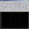
Based on a recent conversation about FETs, I was thinking something along the lines of:
Proposed Power Wiring.jpg


The design goal is to have zero current draw when the switch is OFF and to have minimal (almost none) to enable the boost circuit when the switch is ON. I was trying to disconnect EN from GND when the gate is connected to a positive voltage. I know from the recent discussion on N-FETs, that a N channel FET is not going to work when wired like above.

I know:
1) Source is GND is 0V
2) EN is connected by a 200K resistor to the battery
2) The gate will vary from floating (bad thing?) when unpowered to 3.0-4.4V when turned on.

LiPo power varies from the battery voltage to the USB charging voltage (should be 3.0-4.4V). It is less than 3.0 the power circuit will not enable and produce 5V.

Is 3.0V Vgs enough to enable the FET fully?

Would this work? Other options?
 
I'll probably get hammered for this, but doesn't a Pmos need the gate to be at ground to turn on?
 
I don't know. I was trying to search online on how to wire a Pmos, but didn't find any examples that really helped me understand. I did find a lot of examples that didn't help.
 
I'll probably get hammered for this, but doesn't a Pmos need the gate to be at ground to turn on?
Sort of. Mosfets are enhancement type. A P-channel Mosfet has its source pin at a positive voltage and is turned off when its gate is at the same voltage. It is turned on when its gate is more negative (maybe at ground) .
An N-channel Mosfet has its source pin at a low voltage (maybe at ground) and is turned off when its gate is at the same voltage. It is turned on when its gate is more positive than its source.

EDIT: If the voltage for the Adafruit is positive then an N-Channel Mosfet must be used and when the switch is turned off a resistor must ground its gate to turn it off.
 
Can I install the PMos with the source connected to EN and the drain connected to GND?

When the switch is open, the gate would be at ground and the source at battery and therefore the FET is on. When the switch is closed, the gate will be at battery or higher and thereby turn the FET off.

Can the FET be installed this way? Something doesn't seem quite right to me, but I havne't used individual FETs much (I can't recall ever, actually).
 
Last edited:
Can I install the PMos with the source connected to EN and the drain connected to GND?
Yes, but then the gate must be -5V to -10V to cause the EN to be grounded.

When the switch is open, the gate (of the P-channel Mosfet) would be at ground and the source at battery and therefore the FET is on.
No, gate is floating and the drain-source diode will be backwards and will conduct.

When the switch is closed, the gate will be at battery or higher and thereby turn the FET off.
No, the drain-source diode will be backwards and will conduct.

Besides, the Li-Po voltage is too low for many Mosfets. An ordinary Mosfet barely turns on when its G-S voltage is 4V and will not conduct enough. A Logic-level Mosfet barely turns on when its G-S voltage is 2V, but then it will not conduct enough when the battery is near 3V. There are some tiny very sensitive Mosfets in products but I have never seen them for sale.
 
No, gate is floating and the drain-source diode will be backwards and will conduct.

This was predicated on the suggestion to add a resistor from gate to ground. Though that solves the floating issue, all the other problems with the idea still make it not work.

Do you have any other ideas?

This is a link to the unit https://www.adafruit.com/products/2465

What I know and/or is required:
-Must be (very) low power when the unit is on and no power when the unit is off.
-EN is connected by a 200K resistor to the battery voltage (different than LiPo, as LiPo is either battery of USB if it is plugged in and/or charging)
-Although Post #1 is simplified, there is also access to the battery voltage and to the USB voltage (I don't think that is useful as it isn't always plugged in)
-To fully power down the unit:
*EN must be connected to GND for the unit to be powered down
*LiPo power to the unit must be open circuit
-A DPST switch is an option, if the second set of contacts does any good, but both sets will be closed when the unit is powered on. I haven't figured out what I can do with them, yet.
 
Isn't it just this simple?

24.png


The simulated SPST closes at 1ms and opens at 2ms
The Bss123 is a tiny NFet with a Vth of 1.6V, which sinks more than enough to pull EN~ low when its gate is at 3V.

As usual, Audio is making a mountain out of a Molehill.

ps: while the circuit I posted does what you asked for back in post #1, I read some of the on-line discussion about the "powerBoost", and I don't think you understand how it works.

read this
 
Last edited:
As usual, Audio is making a mountain out of a Molehill.

That's hard to tell. I'm usually the main culprit in do that.

ps: while the circuit I posted does what you asked for back in post #1

I'm not sure that circuit does.

From the post prior to your simulation:
-To fully power down the unit:
*EN must be connected to GND for the unit to be powered down
*LiPo power to the unit must be open circuit

Or in table format:
Switch--Switch Out/Vg--EN
OPEN----"Floating"--0V
CLOSED--LipoV-----Vbat

In your simulation, when Vout =0V, then EN should be 0V.

I read some of the on-line discussion about the "powerBoost", and I don't think you understand how it works.
In what regard? I have reviewed, tested, and commented on that very post using the module I have in hand. (I have other issues with the LBO, but that is a different story for a different forum)

The module has six pins: (original long version here Module Pinout and Functions)
Summary version:
USB - this is the micro USB 5V power pin. Power from the microUSB port when it is plugged in
BAT - this is the battery input, connected directly to the JST connector. For most Lithium batteries, this will range from 3.0V when near-dead to 4.2V when fully-charged.
VS - this is a switched output, either USB when connected or battery power when not connected to USB.
GND - this is the power ground. This boost converter is not 'isolated' - the ground input is the same as the ground output
5V - this is the boosted output. \
EN - this is the 'enable' pin. By default it is pulled 'high' to VS (according tot he schematic it is pulled to battery?). To turn off the booster, connect this pin to ground.
LBO - Low Battery Output. By default it is pulled high to BAT but when the charger detects a low voltage (under 3.2V) the pin will drop down to 0V.

To minimize losses due to regulation, part of the unit runs from VS (Vshared) and the sensor runs from the boosted 5V. To turn the circuit off, but still be able to charge the battery, there needs to be a disconnect between VS and the load. The same does not (completely) apply to 5V. I can turn off the sensor by disconnecting 5V from the sensor, but the booster still runs and draws current. To stop the boost circuit, EN is connected to GND. In short that is how the module works.
 
Last edited:

Attachments

  • 24a.png
    24a.png
    24 KB · Views: 106
Then it is even simpler...

I guess not. I tried and it didn't work (although I used a 1N914 because I don't have any schotkeys on hand). I don't think your simplified PowerBoost is correct. What pulls down EN when the switch is off? Where is the pull up resistor in the PowerBoost? I think EN should be connect between V2 and R2.
 
Last edited:
The load(s) have to be there to act as a pull-down. You said you thought there was a pull-up on EN inside the power-boost. It is easy to tell using a voltmeter. Since EN is a logic input, then the Si diode should work.
 
In trusting and believing you. I tried again. The local electronics store stocks a limited number of NTE parts. I found a NTE180 listed as a schottky diode. I tried again. There was vague success, as the powerboost indicator LED did not turn completely of. I don't think the pull down was hard enough (or too much loss in the diode).

(I find the naming in this schematic very confusing as well as some of the crossed lines)

Powerboost pullup.jpg

There is a pullup resistor from EN to the shared voltage out. So EN is a few mV lower than the shared voltage out. Realizing (not quite understanding) where you were headed with diode. I have to ask, why the diode? Why not just a direct connection?

Final Wiring.jpg
 
Last edited:
Status
Not open for further replies.

Latest threads

New Articles From Microcontroller Tips

Back
Top