Continue to Site

Welcome to our site!

Electro Tech is an online community (with over 170,000 members) who enjoy talking about and building electronic circuits, projects and gadgets. To participate you need to register. Registration is free. Click here to register now.

  • Welcome to our site! Electro Tech is an online community (with over 170,000 members) who enjoy talking about and building electronic circuits, projects and gadgets. To participate you need to register. Registration is free. Click here to register now.

question about crystal oscillator pcb?!

Status
Not open for further replies.

emb

Member
Hi everybody ,

I have finished drawing the layout of my circuit..

my question about crystal oscillator layout .. should i do any modification on it ?

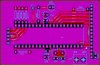
the board 2 sides ..

top (component side) it includes power plane (5V)>>RED color
Untitled3.png


bottom includes ground plane and signal traces >>blue color

Untitled2.png


top and bottom view

Untitled1.png


I want to print the board in my house .

regards :)
 
It is important to get C1,C2 ground back to pin 12 very fast. (short wire) (high frequencies)
I added a red circle. At the center is a thin spot in the copper. When you make a home made board this might brake open. Please make this ground stronger. Move C1 to the right a small amount. OR rotate C1 180 degrees.
upload_2017-8-27_6-37-45.png

Hear what Pommie said.
You will not have "VIAs" in your board. "Feed throughs"
You will also not have solder mask. This makes surface mount harder to solder.
I think you must make one board. It is a good place to learn.
If you lived near me; you could have my chemicals. Maybe they are too old. I have not made boards in a long time.
 
Here are my personal preferences.
1) I make double-sided PCB's at home when I am in a hurry. I do not do that very often lately, as send out is so cheap. However, I recently resurrected my chemicals, and the process still worked fine. I use a pre-sensitized board with a positive-acting photoresist. Getting alignment is easy. I just tape the top and bottom masks as a sleeve and put the board in between. IMHO, double sided is only marginally more difficult than single-sided with that method. In fact, I do not have any single-sided PCB blanks. The only added difficult is in etching as you may need to flip the board to get even etching on both sides.
2) Unless I have a specific reason to use a power plane and ground plane on opposite sides, I do not do that. A rough calculation will show that a 10 cm x 10 cm board on 2 mm FR4 will have about 200 pF from the planes. Usually, I keep a ground plane on both sides, and of course, usually make my power traces larger than signal traces and appropriate for the current.
3) I stitch the two ground planes together with short pieces of wire. Here's a board a made a few weeks ago. It is about 1" on a side.
TOP
upload_2017-8-27_9-41-41.png

BOTTOM
upload_2017-8-27_9-42-54.png


The bottom shows the stitching better. I just drill a fine hole and use 24 awg bare wire for the contact. The hole is small enough to hold the wire for soldering. No bends or crimps are needed. The board looks a little sloppy as it has had several modifications as I adjusted feedback resistors.

4) I do not pay particular attention to SMD or TH components and often have mixed types on a board; although, I prefer SMD, because there are no holes to drill. This board is all SMD, except for the supply pinheader. You can usually solder a TH component on either the component side, opposite side, or both sides, if needed.
 
thank you all for your effort :)

usually we print the board in pcb lab in our university with a very good quality board (single or double sides) ^^
this time i want to print the board in my home for the first time ^.^
but for best quality i will return back to university pcb lab .

i moved c1 as ronsimpson recommend ,,,

now i have two layouts,which one of them recommend me to use ?and if there is any modification :)

regards

rtr.jpg


the second one
ttr.jpg
 

Attachments

  • rtrr.jpg
    rtrr.jpg
    404.7 KB · Views: 229
I assume that you can't do through hole plating and wonder how you will solder the vias under the chip and connections under components like C4.

Mike.
 
usually i put conductor through via and then solder it from bottom and top ^^
i will use socket under the chip ,,,

components like C4 i will solder one leg on top and the other on bottom

for J3 i will not use terminal block i will solder the + 5V and 0V wires directly ^^

sorry for bothering you guys o_O
 
Just FYI, the type of via I described fits nicely under a TH chip, assuming your diagonal cutters are decent. As for J3, I have soldered TH components on the component side many times, even when the fully seated component interferes with access from the soldering iron.. Just raise the component enough off the board to solder its pin(s). Then heat the pins from the bottom to "walk" it down. For up to four pins (e.g., a bridge rectifier) that works easily. I have not tried larger. Imagine that it is a little like using solder paste where you depend on the surface tension to maintain a good joint.

John

thank you john :)
Helpful and valuable comment :)


so what is the better layout the 1st or the second one ?

:)
 
What is the processor, and what is the crystal frequency? You may need a parallel resistor if the processor doesn't include one. You may also need a resistor in series with the output pin to reduce stop overtone oscillation.

Also, I would suggest you turn the capacitors around, and have the capacitors with their ground connections on the outside, and the crystal connections closer together. That keeps the crystal connections further from other circuitry.

Or just use and oscillator and layout is largely unimportant.
 
What is the processor,
Pic16f877a

and what is the crystal frequency?
20Mhz

You may need a parallel resistor if the processor doesn't include one.
Parallel resistor connected with what ?

You may also need a resistor in series with the output pin to reduce stop overtone oscillation.
Output pin of the oscillator ?

Also, I would suggest you turn the capacitors around, and have the capacitors with their ground connections on the outside, and the crystal connections closer together. That keeps the crystal connections further from other circuitry.
I didn't understand this point o_O

Or just use and oscillator and layout is largely unimportant.

Thank you for your reply ;)
 
A parallel resistor would be in parallel with the crystal. I don't think that it is needed with a 16F877A, because that processor contains a resistor, shown in figure 6-2 of the data sheet. (https://ww1.microchip.com/downloads/en/DeviceDoc/39582C.pdf)

The two oscillator pins, T1OSI and T1OSO, are input and output of an inverter. For low frequency crystals, 10 MHz and less, it can be a good idea to put a resistor in series with the output pin. At 20 MHz it's not needed.

Your four capacitor pins are in a row. If you number from one end, 1, 2, 3, 4, you have pins 2 and 3 as ground. I was suggesting having pins 1 and 4 as ground and 2 and 3 as the ones connected to the crystal.

thank you for helpful info ^^

here is the layout after modification
jhy.jpg


and here is the schematic ..
ffg.jpg


I want to use 5v 1A power supply

f44d8008-36ef-4b14-ba56-ce4f71cb33a7.jpg


Regards :)
 
OK, now make it and welcome to the club. I find it quite enjoyable to watch the copper dissolve away.
 
what is the type of decoupling capacitor ?
what is the type of capacitor used with crystal ?

would ceramic type be fine ?


sorry for bothering you guys :)

And thank you for your appreciated effort ;)
 
Ceramic capacitors are often used for both, but decoupling capacitors will be more than 2000 times bigger in capacity. That is 40 pF for the crystal and 0.1 uF (100,000 pF) for decoupling. One will also see larger capacitors or various chemistry (e.g, polyester or electrolytic) used in parallel with a ceramic cap for decoupling.

John

thank you john :)

how can i determine the suitable value of the capacitor for 20Mhz ?
 
A parallel resistor would be in parallel with the crystal. I don't think that it is needed with a 16F877A, because that processor contains a resistor, shown in figure 6-2 of the data sheet. (https://ww1.microchip.com/downloads/en/DeviceDoc/39582C.pdf)

what is the value of parallel resistor ?


The two oscillator pins, T1OSI and T1OSO, are input and output of an inverter. For low frequency crystals, 10 MHz and less, it can be a good idea to put a resistor in series with the output pin.

what is the value of series resistor ?


At 20 MHz it's not needed.

Your four capacitor pins are in a row. If you number from one end, 1, 2, 3, 4, you have pins 2 and 3 as ground. I was suggesting having pins 1 and 4 as ground and 2 and 3 as the ones connected to the crystal.
 
A recommended capacitor size is usually in the specifications for the crystal. If not, assume it is in the 10 pF to 47 pF range. Too much capacitance will overdrive the crystal (also mentioned above). Measuring the actual frequency can be difficult. If you have a good HF receiver, you might pick up the frequency with a small antenna nearby.

What I have done recently is use TMR1 as a frequency counter and a calibrated source. I then changed the crystal/resonator capacitor for the MCU slightly to tune it. Crystal tolerance was specified as +/- 0.5%. I wanted it to be closer. For most cases, changing that will not be necessary.

Here's a more detailed discussion: https://blog.adafruit.com/2012/01/24/choosing-the-right-crystal-and-caps-for-your-design/
 
Status
Not open for further replies.

Latest threads

New Articles From Microcontroller Tips

Back
Top