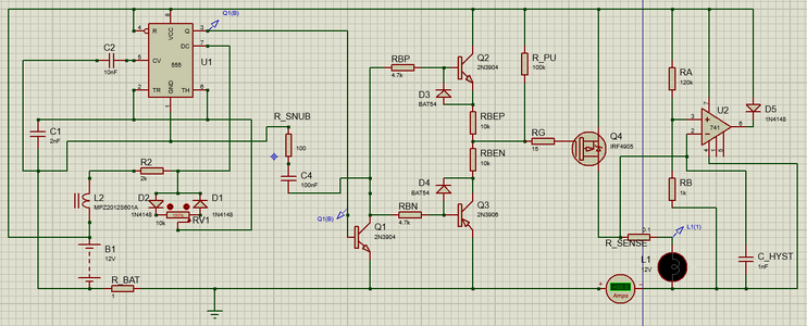
Q3 is upside down as well, collector and emitter are swapped!. The emitter resistors are also far too high at 10K, and not really needed at all.
In fact the whole drive stage is wrong, and won't work - I'm on holiday in Scotland at the moment, otherwise I'd post the driver circuit I use - I'll do it when I get back.
The whole point of the driver is to switch the FET ON and OFF as quickly as possible, which your circuit won't do - there's not even any base bias for Q2, D3 and D4 aren't needed, nor are the four resistors.
Where your Q1 is I use a 2N7000 FET, then there's two resistors in series to the power supply from the drain, and the two driver bases connect directly to the mid point of those two resistors - values in the hundreds of ohms, and the ratio depending on the supply voltage. I use the same circuit with 24V and 12V inputs, and it just needs the resistor ratio tweaking. This is in switch-mode PSU/Charger designs, but the exact same reasons apply.