Continue to Site

Welcome to our site!

Electro Tech is an online community (with over 170,000 members) who enjoy talking about and building electronic circuits, projects and gadgets. To participate you need to register. Registration is free. Click here to register now.

  • Welcome to our site! Electro Tech is an online community (with over 170,000 members) who enjoy talking about and building electronic circuits, projects and gadgets. To participate you need to register. Registration is free. Click here to register now.

power amplifier biasing

Status
Not open for further replies.

hanhan

Member
Hi,
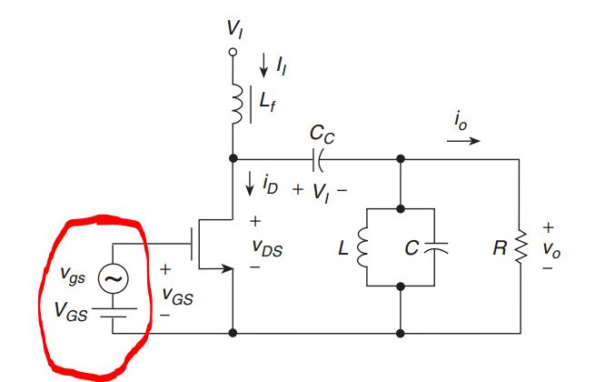
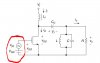
I want to ask a question about the power amplifier biasing.
In this picture the signal and bias sources are connected in series without coupling capacitor.
I heard somewhere that this way of biasing is only theoretical not practical.
Could you tell me why we can't implement the biasing in reality?
theoretical-coupling-power-amplifier-jpg.75146
 

Attachments

  • theoretical coupling power amplifier.JPG
    theoretical coupling power amplifier.JPG
    28.3 KB · Views: 463
Hi,

One reason is that Vgs is not constant over temperature.

Another reason is that the transistor is not linear. If you can get away with the non linearity though you might get it to work.
 
Hi,
I don't quite understand what you said. Can you explain it in more detail.
One reason is that Vgs is not constant over temperature.
Did you mean the threshold voltage Vt? And if so how can we resolve that?
Another reason is that the transistor is not linear. If you can get away with the non linearity though you might get it to work.
I really don't get this. I know that transistor is not linear but why it is related to the question above assuming that VGS is chose so that transistor operates in active region.
 
The arrangement is impractical because the bias circuit is in series with the driver circuit. It is normally the case that the bias circuit is parallel to the the drive circuit so that the bias can be connected with the drive circuit disconnected. A failure in either circuit device will upset the DC conditions and possibly cause damage.
 
Hi,
I don't quite understand what you said. Can you explain it in more detail.

Did you mean the threshold voltage Vt? And if so how can we resolve that?

I really don't get this. I know that transistor is not linear but why it is related to the question above assuming that VGS is chose so that transistor operates in active region.

Hi,

Yes i meant the threshold voltage VT. Since it varies with temperature the bias could change quite a bit. The resolution is to provide feedback for biasing rather than some sort of constant bias.

The transistor is not linear even in the active region. By linear i mean the more precise definition not just that it is not clamped to either ground or +Vcc. The more precise definition of linear is that if for an input x we get y as output, then for an input A*x we get A*y as output. However, this definition can be relaxed to include an input and/or output offset too.
 
Hi,
Yes i meant the threshold voltage VT. Since it varies with temperature the bias could change quite a bit. The resolution is to provide feedback for biasing rather than some sort of constant bias.
I didn't know it. In my textbook they talk a little bit about Vt but it only mentions about the variation of Vt when VSB (the voltage between source and body of MOSFET) non-zero.
 
Status
Not open for further replies.

Latest threads

New Articles From Microcontroller Tips

Back
Top