Continue to Site

Welcome to our site!

Electro Tech is an online community (with over 170,000 members) who enjoy talking about and building electronic circuits, projects and gadgets. To participate you need to register. Registration is free. Click here to register now.

  • Welcome to our site! Electro Tech is an online community (with over 170,000 members) who enjoy talking about and building electronic circuits, projects and gadgets. To participate you need to register. Registration is free. Click here to register now.

PIR to Arduino and LEDs #2

Status
Not open for further replies.
Hello Electro Tech Online Forum,

Its been a while since have been on the forum.
Had to wait for the PCBs to get from Minnesota to Texas.
Then I had a couple honey-do's but I am finally back
in the saddle.

To provide context here is the system complete.
It has been named PODACAL as an acronym of
PIR Optocoupler Arduino DMOS Array LED.
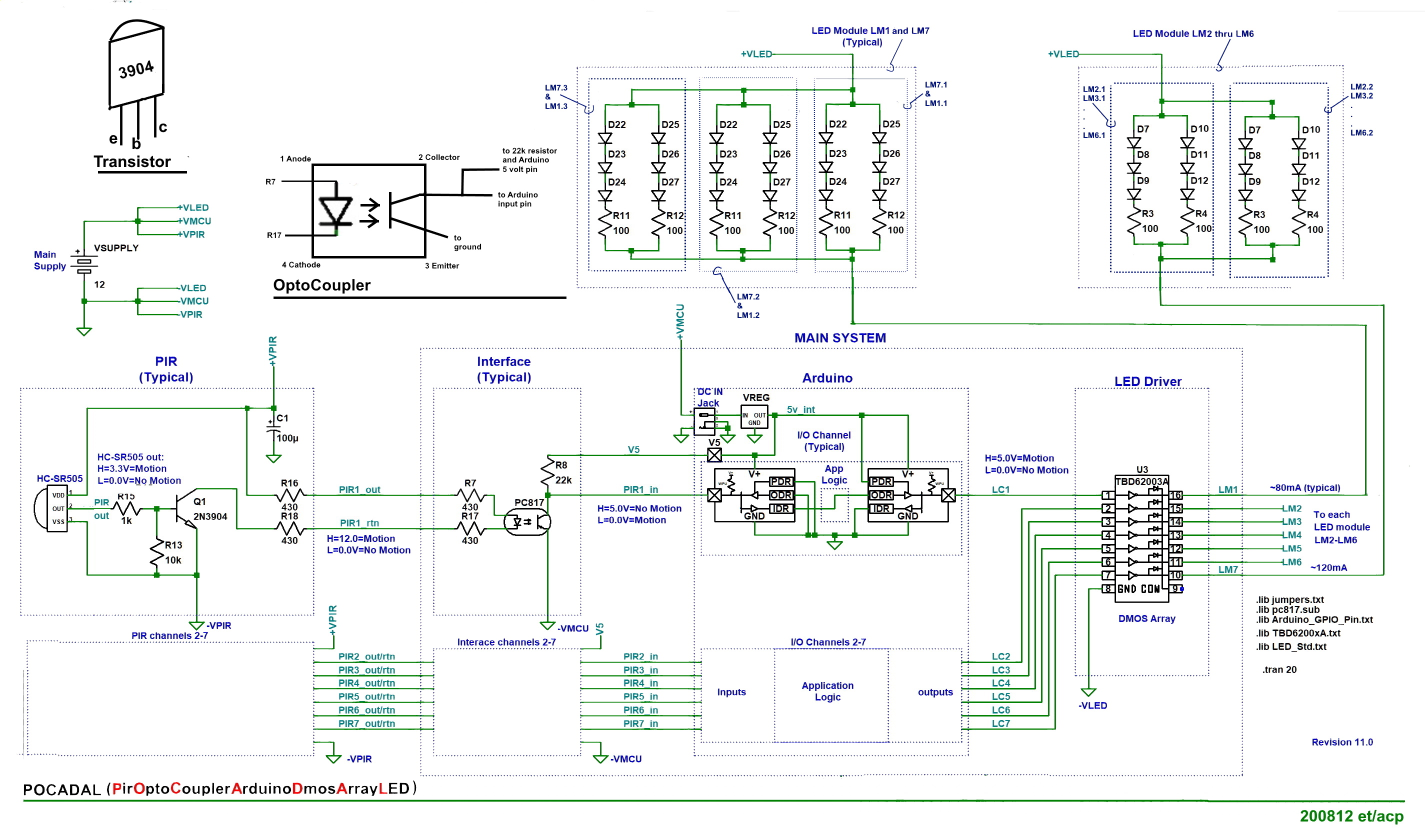
PODACAL_12v_complete_201019.jpg


The excellent schematic by eTech separates
the system into three subsystems or modules:
The LED Module
The Sensor Module
and the
Main Module.

One channel of the system complete has been
tested with the Arduino has been breadboard
tested and works as designed.

The LED Module PCB was tested
and works as designed.

Having a little trouble with the Sensor
Module. Here's the PCB
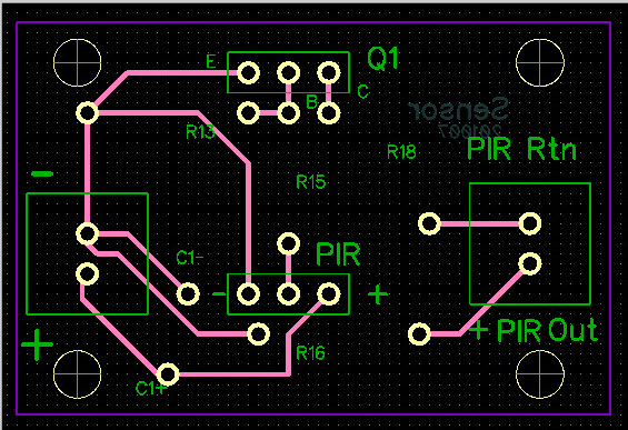
Sensor_Mod_201007.jpg


and drawing with components shown on
the board that is a little easier to read.
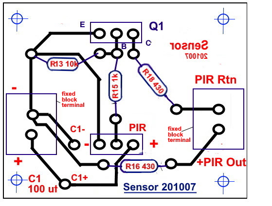
Sensor_Mod_201007_w_components.jpg


These are the test performed

Test 1.
DC voltage at the power source fixed block terminal
DC ground power source fixed block terminal
Expected result: 12 volts
Actual result: 12.4 volts

Test 2.
DC voltage on the PIR out side of R15
DC ground power source fixed block terminal
Expected result before movement near PIR: 0 volts
Actual result before movement near PIR: 0 volts
Expected result after movement near PIR: 3.3 volts
Actual result after movement near PIR: 2.0 volts


Test 3.
DC voltage at fixed block terminal marked +PIR Out
DC ground at fixed block terminal marked +PIR Rtn
Expected result before movement near PIR: 0 volts
Actual result before movement near PIR: -.76 volts
Expected result after movement near PIR: 12 volts
Actual result after movement near PIR: -.01 volts

Test 4.
DC voltage at fixed block terminal marked +PIR Out
DC ground at power source fixed block terminal
Expected result before movement near PIR: 0 volts
Actual result before movement near PIR: 0 volts
Expected result after movement near PIR: 0 volts
Actual result after movement near PIR: 0 volts

So the two highest possibilities are the tests
3 and 4 are incorrect. Or the implementation
of the PCB from the schematic has some fallacy.

Thanks.

Allen in Dallas
 
Last edited:
With four 430R resistors in series with the opto LED you will only get 6mA of current - the datasheet suggests 50mA. However, as I said on your previous thread, I don't understand why this is so complicated. Why not connect the PIR output direct to the Arduino input?

Mike.
 
With four 430R resistors in series with the opto LED you will only get 6mA of current - the datasheet suggests 50mA. However, as I said on your previous thread, I don't understand why this is so complicated. Why not connect the PIR output direct to the Arduino input?

Mike.

Hi mike

As I explained in a previous post, for two reasons, 1)Because the PIR does not output enough voltage to be reliably sensed by the arduino input, and, 2) because we needed some transient protection for the long wires against carpets, rugs, whatever.
The opto's aren't a big a deal. The OP is new to this stuff.

eT
 
Hi Alan,

Looks like R16 is connected incorrectly. One end should connect to PIR_out and the other end to +power supply terminal. Disconnect the end that connects to -power supply and connect it to +power supply.
 
The OP is new to this stuff.
That was kinda my point. Why is there 4 resistors when 1 will do? Why is the LED current only 6mA? Why not use a 3.3V Arduino?

It just seems like overkill but the OP seems happy, so carry on.

Mike.
 
Get rid of all the resistors and the opto.

the PIR already has a base resistor for the 2n3904. If you connect that to the Arduino's 5v source to the 2n3904, all will be good to convert the PIR 3.3v output to a 5v signal. Since you have a bunch of channels, use 10k to 15k resistors from the 5v arduino supply to each 2n3904 collector.

if you are good at soldering, there is room on the PIR to put an SMD transistor (the 0 ohm jumper on the PIR must be removed)

cheers.


48C5AA69-8044-4E0A-8A96-8050BBF73BF9.jpeg
 
Hello Pommie, eTech and gophert,

The input from Pommie and gophert is appreciated and has been studied.
But the system has been taken so far down the road, through breadboard
and PCBs the plan is to the stay the course with the schematic dated 200812
rather than redesign the system at this stage.

Two questions please
'
1. I eTech's rely, post #3 :
'The opto's aren't a big a deal. The OP is new to this stuff.'
The 'OP' is the other person?

2. Just to be clear the drawing of the Sensor module PCB
is refactored herewith.
Sensor_Mod_201020_w_components.jpg

This correctly reflects the direction given in post #4, right?

Based on feedback will order new sensor PCBS, but looks like
I could, first, take an Exacto blade and cut the trace between R16
and the ground fixed block terminal. And second, run a jumper
wire between R16 and the plus 12v post of the terminal block.
Still going to order new PCBs but this rig would be a way
of testing the refactor.

One last thing, when the sensor board is refactored, the way
POCADAL 200812 (post #1) is read, the output from R18 and
R16 at the posts marked 'PIR Rtn' and '+PIR Out' should be
about twelve volts, right? That is, when the Sensor board is
supplied 12 volts then when the PIR is activated, with ground
probe of the DMM connected to the 'PIR Rtn' post and the plus
DC voltage probe connected to the '+PIR Out' post the reading
should be about 12 volts.

Thanks.

Allen in Dallas
 
But the system has been taken so far down the road, through breadboard
and PCBs the plan is to the stay the course with the schematic dated 200812
rather than redesign the system at this stage.

The design will be ok as is. We already know it will work as designed.

1. I eTech's rely, post #3 :

The 'OP' is the other person?

OP = Original Poster (person).
Some forums use TS = Thread Starter

2. Just to be clear the drawing of the Sensor module PCB
is refactored herewith.
View attachment 127569
This correctly reflects the direction given in post #4, right?

Looks correct.

Based on feedback will order new sensor PCBS, but looks like
I could, first, take an Exacto blade and cut the trace between R16
and the ground fixed block terminal. And second, run a jumper
wire between R16 and the plus 12v post of the terminal block.
Still going to order new PCBs but this rig would be a way
of testing the refactor.

Yes. that would be a good way to test.

One last thing, when the sensor board is refactored, the way
POCADAL 200812 (post #1) is read, the output from R18 and
R16 at the posts marked 'PIR Rtn' and '+PIR Out' should be
about twelve volts, right? That is, when the Sensor board is
supplied 12 volts then when the PIR is activated, with ground
probe of the DMM connected to the 'PIR Rtn' post and the plus
DC voltage probe connected to the '+PIR Out' post the reading
should be about 12 volts.

Thanks.

Allen in Dallas

When no motion is detected, there should be less than 0.7 volts at the base of Q1. This keeps Q1 off.
With Q1 off, there should be about 12.0v at the collector of Q1.

When motion is detected, there should be about 2.0 volts at the base of Q1. This turns Q1 on.
With Q1 on, there should be less than 0.7v at the collector of Q1.

After the board is reworked and with 12 vdc power applied to sensor module:
+ PIR out terminal should read a constant 12 vdc.
( + probe to +PIR out, ground probe to -Pwr terminal on the sensor module)
(12 vdc is present at both ends of R16)

To test the sensor module:

1. Connect a temporary jumper from +PIR out to PIR Rtn.
2. Connect the DMM +probe to either the temporary jumper, or the +PIR out terminal. (make sure the jumper is in place)
3. Connect the DMM ground probe to -PWR
4. Connect 12 vdc power to the +PWR and -PWR terminals.
5. The DMM should read about 12 vdc with no motion detected (doesn't need to be exact).
6. Cause motion to be detected by the PIR (a wave of a hand over the PIR).
7. The DMM should read less than 0.7 vdc with motion detected (doesn't need to be exact).

eT
 
Last edited:
Hello eTech and the ETO forum,

Won't get to test the refactored Sensor module
until Saturday or Sunday because I have this deal
with mortgage company: I work, get paid
and pay them whole bunch of after-tax dollars
and they let me live in my house.

Meanwhile have been studying the schematic of the
Sensor module and comparing it to the excellent
seven-step test plan offered in post #8.
PODACAL_12v_Sensor_mod_schematic_201023.jpg

To paraphrase the test plan: the the outputs from the Sensor
module are connected, the 12v volt power is applied
and at the outward side of R16 the DMM should read
12v (+ or - ) with no signal from the PIR (no motion)
and .7 v (+ or -) when a signal is sent from the PIR.

But looking at the schematic it seems to say at
PIR1 rtn
H=12.0=Motion
L=0.0v= No Motion
(blue font)

So this seems to contradict the test plan.
The test plan says 'no motion 12v' while
the callout on the schematic '12.0=Motion'.

Was the PIR1 rtn callout put on the schematic before it was
changed from 5volt to 12 volt in post #11 of the thread
marked 'PIR to Arduino to Transistor and LEDs'
in mid July?

Or am I misreading the schematic?

Thanks.

Allen in Dallas
 
But looking at the schematic it seems to say at
PIR1 rtn
H=12.0=Motion
L=0.0v= No Motion
(blue font)

So this seems to contradict the test plan.
The test plan says 'no motion 12v' while
the callout on the schematic '12.0=Motion'.

Hi

The "blue font" at the output of the sensor module is incorrect. However, the test plan does need a minor correction
The blue font at the sensor output should read:

H=12.0=No Motion
L=10.0v=Motion

Meaning:
There should be 12.0 vdc when no motion.
There should be <10.0 vdc when motion detected.

The test plan should be updated as follows.

7. The DMM should read less than <7.0 vdc with motion detected (doesn't need to be exact).

The sensor module output voltage will be different for the module test because we are using a jumper between the +PIR_out and PIR_rtn.
 
Last edited:
Hello eTech and the ETO forum,

Finally got the chores done and got back to the bench.

Refactored the Sensor PCB, loaded it up and performed the
seven step test.

The outcome from the no-motion test is as expected, 12.39 volts.
Sensor_7_53_600_800.JPG

However the read out from the nine seconds after motion is detected is 7.53, not .7 (plus or minus) that was expected.

It was conjectured that some mistake had been made. A second board was loaded.
Using a one sixteenth inch drill bit with a hand tool the R16 is disconnected from the voltage plus terminal.
Sensor_hack_201025_600_800.JPG


It was checked to make sure there was no continuity between R16 and ground.
Found the lead from R16 could be insulated and connected to the V+ power fixed terminal.
Sensor_back_201025_2_600_800.JPG


This is how the board looks with with all parts loaded except the PIR and the capacitor so the PCB can be seen before the cap and the PIR obstruct the view.

Sensor_wo_cap_201025_600_800.JPG


Performed the test on the second board:

Ground probe at power source ground and +voltage probe connected to the
jumper between PIR Rtn and +PIR Out, before movement at PR.
Expected result: 12 volts
Actual result: 12.39 volts


Ground probe at power source ground and +voltage probe connected to the
jumper between PIR Rtn and +PIR Out, after movement at PR.
Expected result: .7 volts (+ or-)
Actual result: 7.83 volts

It seems like the difference between .7 and 7.53 or 7.83 is not within tolerances.

So guess maybe the same mistake was made on both boards. Have checked to make sure that the
PCB shown in the photo above marked 'OCADAL (PirOptoCouplerArduinoDr' matches the
drawing of the board titled 'Sensor 201020' shown in post #7.

Thanks.

Allen in Dallas
 
I don't understand how you expect 0.7V with the voltage divider network you set up. I showed you how to get to get your low active in post 6.

here is the simple ohms law review of your design (voltages in red).

15381DAD-E8E0-4628-82C5-D577DCDBBBA2.jpeg
 
Hello gophert, eTech and the ETO forum,

Ok I got a little confused. Post #8 indicated
7. The DMM should read less than 0.7 vdc with motion detected (doesn't need to be exact).

But then in post # 10 step seven was updated

7. The DMM should read less than <7.0 vdc with motion detected (doesn't need to be exact).

So the 7.53 reading means the Sensor modules are performing as designed.
Staircase_Main_Board_201024_w_comps.jpg

So the Sensor modules go into the main board at the fixed terminal blocks
S1 thru S8

The fixed terminal blocks LM1 thru LM7 go out to the ground sides of the
LED modules.

Need to think thru the logic used to design the main board a couple of months
ago. Its getting late and having a hard time figuring out the rationale.

Thanks.
'
Allen in Dallas
 
It looks like your supply is ~12.5V and you have a voltage divider to give you half the voltage from 12.5 to the collector of the transistor. As you're getting 5V across the top resistor (12.5-7.5) then you should have the same across the bottom one which suggests you have 2.5V across the transistor. Can you measure across the transistor?

Mike.
 
Before I comment, be aware that when I state measurements, I'm working on a bench with a breadboarded circuit. The bench power supply is initially adjusted to 12.0 vdc without load, then re-adjusted for 12.0 vdc after connecting the load.

You should do the same before making measurements.

Hello eTech and the ETO forum,

Finally got the chores done and got back to the bench.

Refactored the Sensor PCB, loaded it up and performed the
seven step test.

The outcome from the no-motion test is as expected, 12.39 volts.
View attachment 127654
However the read out from the nine seconds after motion is detected is 7.53, not .7 (plus or minus) that was expected.

7.53 volts is a little high but OK. There will be tolerance differences between your parts, test bench, and mine.
Even the solder joint quality can make a difference. Poor quality joints can raise resistances and drop less voltage than expected.

It was conjectured that some mistake had been made. A second board was loaded.
Using a one sixteenth inch drill bit with a hand tool the R16 is disconnected from the voltage plus terminal.

I think you mean "minus" terminal.

View attachment 127655

It was checked to make sure there was no continuity between R16 and ground.
Found the lead from R16 could be insulated and connected to the V+ power fixed terminal.
View attachment 127656

This is how the board looks with with all parts loaded except the PIR and the capacitor so the PCB can be seen before the cap and the PIR obstruct the view.

View attachment 127657

Performed the test on the second board:

Ground probe at power source ground and +voltage probe connected to the
jumper between PIR Rtn and +PIR Out, before movement at PR.
Expected result: 12 volts
Actual result: 12.39 volts

12.39 ok.

Ground probe at power source ground and +voltage probe connected to the
jumper between PIR Rtn and +PIR Out, after movement at PR.
Expected result: .7 volts (+ or-)
Actual result: 7.83 volts

It seems like the difference between .7 and 7.53 or 7.83 is not within tolerances.

So guess maybe the same mistake was made on both boards. Have checked to make sure that the
PCB shown in the photo above marked 'OCADAL (PirOptoCouplerArduinoDr' matches the
drawing of the board titled 'Sensor 201020' shown in post #7.

No mistake. 7.83 volts is a little high but OK. That is close enough to the expected results of <7.0v

My "sensor module" test readings:

PWR: 12.0 vdc

Volts at jumper:
no motion=12.0 vdc
motion detected=6.01 vdc

Volts at Q1 Collector to gnd:
no motion=12.0 vdc
motion detected=68.0 mvdc
 
Last edited:
Here are my bench measurements for the sensor module with jumper in place. Power supply is set to 12.0 vdc

1603677982745.png
 
Last edited:
Hello gophert, eTech and the ETO forum,

The Arduino Shield Main Board for the Staircase project
was designed over a month ago. Last night when the
Sensor module was tested positive a look at the at
the Main board/shield was taken to begin connecting the Sensor modules
and LED modules for staircase mockup.

There were several things that did not make any sense
on the PCB marked 'POCADAL Main Board 201024' in
Staircase_Main_Board_201024_b.jpg

post # 13 above and copied here. Among other things what is the function
of the terminal blocks (six positions at top
and three positions beneath) to the left of
pads numbered vertically from 2 to 10?

Today, Monday I had the day off from work so
'POCADAL Main Board 201024' shown in post # 13
was studied to make sure it was an implementation
of the schematic dated 201012 in post #1 of this thread.
This is a sort of a schematic/PCB drawing used to
analyze the schematic deployment to a PCB.
PODACAL_12v_Arduino_Shield_Main_Board_201026.jpg


Today it was realized that in late Aug in the thread
called PIR to Arduino to Transistor and LEDs
at post #48 eTech suggested that the
Link to PIR to Arduino to Transistor and LEDs post #48
opto-couplers be moved from the Sensor modules
to the Shield/Main board because the function
of the opto coupler is to reduce EMI in
the long runs between the Sensors and the
Shield. So the FTBs (fixed terminal blocks)
at the headers going thru pads 2 to 10
to the Uno were obviated by the FTBs
marked S1-S8 near the 430 ohm resistors.
That is, the FTBs on the Sensors modules
were moved to the Shield but I forgot
to remove the FTBs designed to receive
the wires from the sensors.

Other 'Oh shoots' and 'I-don't-
believe-I made -such-dumb-ass -
mistake's' were found and refactored.

So if you have a chance, please
check out the the drawing marked
POCADAL Arudino Shield and Main Board
201026 posted herewith above.

Especially concerned about the connection
of the opto-coupler collector connection to the Arduino
5v supply via R8 22k resistor.

In building a shield for the Arduino
one of the toughest parts was getting
the pads in the PCB to line up with the pin
headers on the Arduino. It took
a set of digital calipers and a lot of time
but the alignment was achieved. What
was missed was the top of the USB
port and the power barrel jack is
higher than the pin headers. That is why
in the PCB drawing in post #13
('POCADAL Main Board 201024') there
are two leave-outs at the bottom of the board
between S4 and S5 and between S6 and S7.

The plan is to based on the always excellent
feedback from the ETO forum, redesign 'POCADAL Main Board 201024'
this Saturday and re-order a new board.

Thanks.

Allen in Dallas
 
Last edited:
Hello gophert, eTech and the ETO forum,

The Arduino Shield Main Board for the Staircase project
was designed over a month ago. Last night when the
Sensor module was tested positive a look at the at
the Main board/shield was taken to begin connecting the Sensor modules
and LED modules for staircase mockup.

There were several things that did not make any sense
on the PCB marked 'POCADAL Main Board 201024' in
View attachment 127671
post # 13 above and copied here. Among other things what is the function
of the terminal blocks (six positions at top
and three positions beneath) to the left of
pads numbered vertically from 2 to 10?

Today, Monday I had the day off from work so
'POCADAL Main Board 201024' shown in post # 13
was studied to make sure it was an implementation
of the schematic dated 201012 in post #1 of this thread.
This is a sort of a schematic/PCB drawing used to
analyze the schematic deployment to a PCB.
View attachment 127670

Today it was realized that in late Aug in the thread
called PIR to Arduino to Transistor and LEDs
at post #48 eTech suggested that the
Link to PIR to Arduino to Transistor and LEDs post #48
opto-couplers be moved from the Sensor modules
to the Shield/Main board because the function
of the opto coupler is to reduce EMI in
the long runs between the Sensors and the
Shield. So the FTBs (fixed terminal blocks)
at the headers going thru pads 2 to 10
to the Uno were obviated by the FTBs
marked S1-S8 near the 430 ohm resistors.
That is, the FTBs on the Sensors modules
were moved to the Shield but I forgot
to remove the FTBs designed to receive
the wires from the sensors.

Other 'Oh shoots' and 'I-don't-
believe-I made -such-dumb-ass -
mistake's' were found and refactored.

So if you have a chance, please
check out the the drawing marked
POCADAL Arudino Shield and Main Board
201026 posted herewith above.

Especially concerned about the connection
of the opto-coupler collector connection to the Arduino
5v supply via R8 22k resistor.

In building a shield for the Arduino
one of the toughest parts was getting
the pads in the PCB to line up with the pin
headers on the Arduino. It took
a set of digital calipers and a lot of time
but the alignment was achieved. What
was missed was the top of the USB
port and the power barrel jack is
higher than the pin headers. That is why
in the PCB drawing in post #13
('POCADAL Main Board 201024') there
are two leave-outs at the bottom of the board
between S4 and S5 and between S6 and S7.

The plan is to based on the always excellent
feedback from the ETO forum, redesign 'POCADAL Main Board 201024'
this Saturday and re-order a new board.

Thanks.

Allen in Dallas


What PCB layout software are you using to design the board?
Does it have a matching schematic capture program as well?

May be a little late in the game but I ask these questions because if the schematic was captured with the software, then design changes could be sent back and forth between the schematic and board layout to keep them synchronized, making change management a lot easier. If you make a mistake, you could make the correction in one process and easily pass the changes to the other process.

As a suggestion,
Make one schematic of each module. This will be used as a main copy.
Make one board layout for each module. This will be used as a main copy.
Make one system diagram showing each module and how they interconnect. This should include any third party components like the Arduino, Power Supply, and power distribution. This will also be used as a main copy.
Each of these documents will grow in detail as the design progresses, and should be updated regularly. Their content supersedes any other versions.
Keep a record of any major change to any of these documents. These can be in the form of electronic notes, or printed copies.
The records will create a "history" you can refer to in the event the reason for a change cannot be deduced.

Anyway, I'll take a look at your newly posted drawing.
 
Last edited:
Hello

I've reviewed your drawing. I had some trouble making out the connections on DWG 201026 so I made my own. Please review attached for the following comments.

1. R8 at the left side of 201026 is not needed.
2. All resistors on this module can be 1/4W, 5%.
3. I've added feed thru terminals to connect to the Arduino supplied 5V and GND

Hope what I've shown makes sense.
1603915971269.png
 
Hello eTech and the ETO forum,

Response to post #18:

The PC layout software is Dip Trace by Novarm
Link to Dip Trace home page
It does have a Schematic Capture module.
An attempt to master the Schematic Capture
feature was attempted but was abandoned in the face of a steep
learning curve. But now that a comfort level
has been achieved with the PCB Layout domain
will look at using the Schematic Capture.
I can see, not only would it save time, but solve
issues at several levels in going from schematic to PCB.

Will repost all three module schematics and
PCBs.

Have had some years of element versioning
working with software. It may be noticed
that the drawings are always dated and some have
revision notes like POCADAL Sensor Module
PODACAL_12v_Sensor_mod_schematic_201023.jpg

dated 200725 revised in Aug and Oct.
Although it is admitted sometimes revisions
are not always noted and will double down
on that.

Response to post #19:
Will post separate LED, Sensor and
Shield schematic and PCBs as soon as able.

I believe this is the latest over all schematic.
PODACAL_12v_complete_201024.jpg

Was there another schematic of the complete
system posted? It was thought that this
is the latest. The bread board was
examined and there is a red/red/orange
resistor. But i guess it was eliminated
and the elimination was missed.

Oh, wait a minute. Separate 22k resistors
are shown for each of the sensor inputs
on schematic marked 'REF: 202026 Rev 2020/1028'.
They are marked R1, R2, R3, R4, R5, R6, R15, R25.

So in preparation for refactoring the
Shield Main Board would just run through
some of the ideas about how the Sensors
connect to the Main Board Shield and the
Arduino underneath. (It is realized that
pins from the shield penetrate down from the shield
to the Arduino for inputs on the left and
for outputs from the Arduino to the
DMOS array IC on the right. Right?)

1. The wires (some of them several feet long)
go from the two position fixed terminal blocks
(FTBs) on the Sensor modules and are received by
two position FTBs on the Shield marked
'IN S1 RTN' thru 'IN S8 RTN' on schematic
marked 'REF: 202026 Rev 2020/1028'.

2. The 'IN S1 RTN' FTBs go to sixteen 430 ohm
resistors and to the anode and cathode of the
optocouplers. The emitters of the optocouplers
go to ground. The optocoupler collectors
go first, via traces on the shield, to the
Arduino input pins, and second to a 22k
resistor and then to the plus five volt
pin of the Uno.

This is the only part that made me scratch my
head. 'REF: 202026 Rev 2020/1028' shows what
is designed on the shield to be header pins
going thru shield down to the Arduino as
FTB1 and FTB2 (FTBs?)
Beginning to think this just how the headers
are marked based on the mistake I made in the PCB
marked 'POCADAL Arduino Shield Maon(sic) 201024
in post #17. That is, an extra set of FTBs were
shown because I forgot to remove
the FTBs from the shield when the optocouplers
were moved to the shield.

This is probably the same reason why the six input pins
sticking down thru the shield to pins A0-A5
on the Arduino are marked FTB3. My bad.

Ok I get it. The big difference between
'REF: 202026 Rev 2020/1028' and the two
drawings in post #17 ('POCADAL...201024'
and 'POCADAL...201026) is my drawing
shows one 22k resistor and eTech's shows
eight 22k resistors.

Will
1. Post the latest schematics and PCB
drawing of the LED and Sensor modules.

2. Redraw the shield PCB drawing based on
'REF: 202026 Rev 2020/1028' and post.

Glad I got your input before I ordered
the shield PCB.

Thanks.

Allen in Dallas

PS Sorry about the length of this post
but I think it got us on the same path.
 
Status
Not open for further replies.

New Articles From Microcontroller Tips

Back
Top